Propagation Delay


What is propagation delay: Propagation delay of a logic gate is defined as the time it takes for the effect of change in input to be visible at the output. In other words, propagation delay is the time required for the input to be propagated to the output. Normally, it is defined as the difference between the times when the transitioning input reaches 50% of its final value to the time when the output reaches 50% of the final value showing the effect of input change. Here, 50% is the defined as the logic threshold where output (or, in particular, any signal) is assumed to switch its states.


2 input AND gate
Figure 1: 2-input AND gate

Propagation delay example: Let us consider a 2-input AND gate as shown in figure 1, with input ‘I2’ making transition from logic ‘0’ to logic ‘1’ and 'I1' being stable at logic value '1'. In effect, it will cause the output ‘O’ also to make a transition. The output will not show the effect immediately, but after certain time interval. The timing diagram for the transitions are also shown. The propagation delay, in this case, will be the time interval between I2 reaching 50% while rising to 'O' reaching 50% mark while rising as a result of 'I2' making a transition. The propagation delay is labeled as “TP” in figure 2.

The propagation delay is the time from 50 percent of transitioning input to 50% of transitioning output
Figure 2: Propagation delay


On what factors propagation delay depends: The propagation delay of a logic gate is not a constant value, but is dependent upon two factors:

  1. Transition time of the input causing transition at the output: More the transition time at the input, more will be the propagation delay of the cell. For less propagation delays, the signals should switch faster.
  2. The output load being felt by the logic gate: Greater is the capacitive load sitting at the output of the cell, more will be the effort put (time taken) to charge it. Hence, greater is the propagation delay.
How Propagation delay of logic gates is calculated: In physical design tools, there can be following sources of calculation of propagation delay:

  • Liberty file: Liberty file contains a lookup table for the each input-to-output path (also called as cell arc) for logic gates as .lib models. The table contains values for different input transition times and output loads corresponding to cell delay. Depending upon the input transition and output load that is present in the design for the logic gate under consideration, physical design tools interpolate between these values and calculate the cell delay.
  • SDF file: SDF (Standard Delay Format) is the extracted delay information of a design. The current delay information, as calculated, can be dumped into SDF file. It can, then, be read back. In case SDF is read, delays are not calculated and SDF delays are given precedence.

Output transition time: The output transition time is also governed by the same two factors as propagation delay. In other words, larger transition time and load increase the transition time of the signal at the output of the logic gate. So, for better transition times, both of these should be less.

Read next : Negative delay- How is it possible


Also read:

Multicycle paths : The architectural perspective


Definition of multicycle paths: By definition, a multi-cycle path is one in which data launched from one flop is allowed (through architecture definition) to take more than one clock cycle to reach to the destination flop. And it is architecturally ensured either by gating the data or clock from reaching the destination flops. There can be many such scenarios inside a System on Chip where we can apply multi-cycle paths as discussed later. In this post, we discuss architectural aspects of multicycle paths. For timing aspects like application, analysis etc, please refer Multicycle paths handling in STA.

Why multi-cycle paths are introduced in designs: A typical System on Chip consists of many components working in tandem. Each of these works on different frequencies depending upon performance and other requirements. Ideally, the designer would want the maximum throughput possible from each component in design with paying proper respect to power, timing and area constraints. The designer may think to introduce multi-cycle paths in the design in one of the following scenarios:
      
       1)      Very large data-path limiting the frequency of entire component: Let us take a hypothetical case in which one of the components is to be designed to work at 500 MHz; however, one of the data-paths is too large to work at this frequency. Let us say, minimum the data-path under consideration can take is 3 ns. Thus, if we assume all the paths as single cycle, the component cannot work at more than 333 MHz; however, if we ignore this path, the rest of the design can attain 500 MHz without much difficulty. Thus, we can sacrifice this path only so that the rest of the component will work at 500 MHz. In that case, we can make that particular path as a multi-cycle path so that it will work at 250 MHz sacrificing the performance for that one path only.
     
     2)      Paths starting from slow clock and ending at fast clock: For simplicity, let us suppose there is a data-path involving one start-point and one end point with the start-point receiving clock that is half in frequency to that of the end point. Now, the start-point can only send the data at half the rate than the end point can receive. Therefore, there is no gain in running the end-point at double the clock frequency. Also, since, the data is launched once only two cycles, we can modify the architecture such that the data is received after a gap of one cycle. In other words, instead of single cycle data-path, we can afford a two cycle data-path in such a case. This will actually save power as the data-path now has two cycles to traverse to the endpoint. So, less drive strength cells with less area and power can be used. Also, if the multi-cycle has been implemented through clock enable (discussed later), clock power will also be saved.

Implementation of multi-cycle paths in architecture: Let us discuss some of the ways of introducing multi-cycle paths in the design:

      1)      Through gating in data-path: Refer to figure 1 below, wherein ‘Enable’ signal gates the data-path towards the capturing flip-flop. Now, by controlling the waveform at enable signal, we can make the signal multi-cycle. As is shown in the waveform, if the enable signal toggles once every three cycles, the data at the end-point toggles after three cycles. Hence, the data launched at edge ‘1’ can arrive at capturing flop only at edge ‘4’. Thus, we can have a multi-cycle of 3 in this case getting a total of 3 cycles for data to traverse to capture flop. Thus, in this case, the setup check is of 3 cycles and hold check is 0 cycle.
Figure 1: Introducing multicycle paths in design by gating data path


    Now let us extend this discussion to the case wherein the launch clock is half in frequency to the capture clock. Let us say, Enable changes once every two cycles. Here, the intention is to make the data-path a multi-cycle of 2 relative to faster clock (capture clock here). As is evident from the figure below, it is important to have Enable signal take proper waveform as on the waveform on right hand side of figure 2. In this case, the setup check will be two cycles of capture clock and hold check will be 0 cycle.
   
   
When the launch clock is half in frequency, it is better to make the path a multicycle of 2 because data will anyways be launched once every few cycles.
Figure 2: Introducing multi-cycle path where launch clock is half in  frequency to capture clock


        2) Through gating in clock path: Similarly, we can make the capturing flop capture data once every few cycles by clipping the clock. In other words, send only those pulses of clock to the capturing flip-flop at which you want the data to be captured. This can be done similar to data-path masking as discussed in point 1 with the only difference being that the enable will be masking the clock signal going to the capturing flop. This kind of gating is more advantageous in terms of power saving. Since, the capturing flip-flop does not get clock signal, so we save some power too.
    
Figure 3: Introducing multi cycle paths through gating the clock path
      Figure 3 above shows how multicycle paths can be achieved with the help of clock gating. The enable signal, in this case, launches from negative edge-triggered register due to architectural reasons (read here). With the enable waveform as shown in figure 3, flop will get clock pulse once in every four cycles. Thus, we can have a multicycle path of 4 cycles from launch to capture. The setup check and hold check, in this case, is also shown in figure 3. The setup check will be a 4 cycle check, whereas hold check will be a zero cycle check.

Pipelining v/s introducing multi-cycle paths: Making a long data-path to get to destination in two cycles can alternatively be implemented through pipelining the logic. This is much simpler approach in most of the cases than making the path multi-cycle. Pipelining means splitting the data-path into two halves and putting a flop between them, essentially making the data-path two cycles. This approach also eases the timing at the cost of performance of the data-path. However, looking at the whole component level, we can afford to run the whole component at higher frequency. But in some situations, it is not economical to insert pipelined flops as there may not be suitable points available. In such a scenario, we have to go with the approach of making the path multi-cycle.

References:


False paths basics and examples

False path is a very common term used in STA. It refers to a timing path which is not required to be optimized for timing as it will never be required to get captured in a limited time when excited in normal working situation of the chip. In normal scenario, the signal launched from a flip-flop has to get captured at another flip-flop in only one clock cycle. However, there are certain scenarios where it does not matter at what time the signal originating from the transmitting flop arrives at the receiving flop. The timing path resulting in such scenarios is labeled as false path and is not optimized for timing by the optimization tool.
Definition of false path: A timing path, which can get captured even after a very large interval of time has passes, and still, can produce the required output is termed as a false path. A false path, thus, does not need to get timed and can be ignored while doing timing analysis.
Common false path scenarios:  Below, we list some of the examples , where false paths can be applied:
Synchronized signals: Let us say we have a two flop synchronizer placed between a sending and receiving flop (The sending and receiving flops may be working on different clocks or same clock). In this scenario, it is not required to meet timing from launching flop to first stage of synchronizer. Figure 1 below shows a two-flop synchronizer. We can consider the signal coming to flop1 as false, since, even if the signal causes flop1 to be metastable, it will get resolved before next clock edge arrives with the success rate governed by MTBF of the synchronizer. This kind of false path is also known as Clock domain crossing (CDC).

The paths to synchronizer are false as the metastability is accounter for
Figure 1: A two flop synchronizer
However, this does not mean that wherever you see a chain of two flops, there is a false path to first flop. The two flops may be for pipelining the logic. So, once it is confirmed that there is a synchronizer, you can specify the signal as false.
Similarly, for other types of synchronizers as well, you can specify false paths.

False paths for static signals arising due to merging of modes: Suppose you have a structure as shown in figure 1 below. You have two modes, and the path to multiplexer output is different depending upon the mode. However, in order to cover timing for both the modes, you have to keep the “Mode select bit” unconstrained. This result in paths being formed through multiplexer select also. You can specify "set false path" through select of multiplexer as this will be static in both the modes, if there are no special timing requirements related to mode transition on this signal. Specifically speaking, for the scenario shown in figure 1,
          Mode 1 : set_case_analysis 0 MUX/SEL
          Mode 2 : set_case_analysis 1 MUX/SEL
          Mode with Mode1 and Mode2 merged together : set_false_path -through MUX/SEL
Select signal selects between two paths for different modes


Figure 2: Mode selection signal selecting between mode1 and mode2 paths
Architectural false paths: There are some timing paths that are never possible to occur. Let us illustrate with the help of a hypothetical, but very simplistic example that will help understand the scenario. Suppose we have a scenario in which the select signals of two 2:1 multiplexers are tied to same signal. Thus, there cannot be a scenario where data through in0 pin of MUX0 can traverse through in1 pin of MUX1. Hence, it is a false path by design architecture. Figure 3 below depicts the scenario.
Figure shows an example of a path that is false by architecture.
Figure 3: A hypothetical example showing architectural false path
Specifying false path: The SDC command to specify a timing path as false path is "set_false_path". We can apply false path in following cases:
  •      From register to register paths
    • set_false_path -from regA -to regB

  •      Paths being launched from one clock and being captured at another
    • set_false_path -from [get_clocks clk1] -to [get_clocks clk2]

  •      Through a signal
    • set_false_path -through [get_pins AND1/B]

Also read:

Setup time and hold time basics

In digital designs, each and every flip-flop has some restrictions related to the data with respect to the clock in the form of windows in which data can change or not. There is always a region around the clock edge in which input data should not change at the input of the flip-flop. This is because, if the data changes within this window, we cannot guarantee the output. The output can be the result of either of the previous input, the new input or metastability (as explained in our post  'metastability'). This window is marked by two boundary lines, one pertaining to the setup time of the flop, the other to the hold time defined as below.

Definition of Setup time: Setup time is defined as the minimum amount of time before the clock's active edge that the data must be stable for it to be latched correctly. In other words, each flip-flop (or any sequential element, in general) needs some time for the data to remain stable before the clock edge arrives, such that it can reliably capture the data. This duration is known as setup time.
The data that was launched at the previous clock edge should be stable at the input at least setup time before the clock edge. So, adherence to setup time ensures that the data launched at previous edge is captured properly at the current edge. In other words, we can also say that setup time adherence ensures that the system moves to next state smoothly. 
Definition of Hold time: Hold time is defined as the minimum amount of time after the clock's active edge during which data must be stable. Similar to setup time, each sequential element needs some time for data to remain stable after clock edge arrives to reliably capture data. This duration is known as hold time.
The data that was launched at the current edge should not travel to the capturing flop before hold time has passed after the clock edge. Adherence to hold time ensures that the data launched at current clock edge does not get captured at the same edge. In other words, hold time adherence ensures that system does not deviate from the current state and go into an invalid state.
As shown in the figure 1 below, the data at the input of flip-flop can change anywhere except within the seup time hold time window. 

Figure showing the setup and hold requirements forming a timing window during which data cannot toggle
Figure 1: Setup-hold window


A D-latch is composed of two inverters, connected in positive feedback loop which is tristated when input data path is enabled. On the other hand, when data path is tristated, this loop is enable
A D-type latch

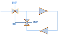
Cause/origin of setup time and hold timeSetup time and hold time are said to be the backbone of timing analysis. Rightly so, for the chip to function properly, setup and hold timing constraints need to be met properly for each and every flip-flop in the design. If even a single flop exists that does not meet setup and hold requirements for timing paths starting from/ending at it, the design will fail and meta-stability will occur. It is very important to understand the origin of setup time and hold time as whole design functionality is ensured by these. Let us discuss the origin of setup time and hold time taking an example of D-flip-flop as in VLSI designs, D-type flip-flops are almost always used. A D-type flip-flop is realized using two D-type latches; one of them is positive level-sensitive, the other is negative level-sensitive. A D-type latch, in turn, is realized using transmission gates and inverters. Figure below shows a positive-level sensitive D-type latch. Just inverting the transmission gates’ clock, we get negative-level sensitive D-type latch.

A complete D flip-flop using the above structure of D-type latch is shown in figure below:

 A D-type flip-flop consists of two latches connected back to back in master-slave format
A D-type flip-flop


Now, let us get into the details of above figure. For data to be latched by ‘latch 1’ at the falling edge of the clock, it must be present at ‘Node F’ at that time. Since, data has to travel ‘NodeA’ -> ‘Node B’ -> ‘Node C’ -> ‘Node D’ -> ‘Node E’ -> ‘Node F’ to reach ‘Node F’, it should arrive at flip-flop’s input (Node A) at some earlier time. This time for data to reach from ‘Node A’ to ‘Node F’ is termed as data setup time (assuming CLK and CLK' are present instantaneously. If that is not the case, it will be accounted for accordingly). Similarly, it is necessary to ensure a stable value at the input to ensure a stable value at ‘Node C’. In other words, hold time can be termed as delay taken by data from ‘Node A’ to ‘Node C’.

Setup and hold checks in a design: Basically, setup and hold timing checks ensure that a data launched from one flop is captured at another properly. Considering the way digital designs of today are designed (finite state machines), the next state is derived from its previous state.  So, data launched at one edge should be captured at next active clock edge. Also, the data launched from one flop should not be captured at next flop at the same edge. These conditions are ensured by setup and hold checks. Setup check ensures that the data is stable before the setup requirement of next active clock edge at the next flop so that next state is reached. Similarly, hold check ensures that data is stable until the hold requirement for the next flop for same clock edge has been met so that present state is not corrupted.

A timing path from rise edge-triggered flip-flop to rise edge-triggered flip-flop
A sample path in a design
Shown above is a flop-to-flop timing path. For simplicity, we have assumed that both the flops are rise edge triggered. The setup and hold timing relations for the data at input of second flop can be explained using the waveforms below:


waveform showing setup and hold requirement for the sample timing path shown above
Figure showing setup and hold checks being applied for the timing path shown above


As shown, data launched from launching flop is allowed to arrive at the input of the second flop only after a delay greater than its hold requirement so that it is properly captured. Similarly, it must not have a delay greater than (clock period – setup requirement of second flop). In other words, mathematically speaking, setup check equation is given as below (assuming zero skew between launch and capture clocks):
                                Tck->q + Tprop + Tsetup < Tperiod
 Similarly, hold check equation is given as:
                               Tck->q  + Tprop > Thold

If we take into account skews between the two clocks, the above equations are modified accordingly. If Tskew is the skew between launch and capture flops, (equal to latency of clock at capture flop minus latency of clock at launch flop so that skew is positive if capture flop has larger latency and vice-versa), above equations are modified as below:
                    
                      Tck->q + Tprop + Tsetup - Tskew < Tperiod
                      Tck->q  + Tprop > Thold + Tskew

Setup checks and hold checks for reg-to-reg paths explains different cases covering setup and hold checks for flop-to-flop paths.

What if setup and/or hold violations occur in a design: As said earlier, setup and hold timings are to be met in order to ensure that data launched from one flop is captured properly at the next flop at next clock edge so as to transfer the state-machine of the design to the next state. If the setup check is violated, the data will not be captured at the next clock edge properly. Similarly, if hold check is violated, data intended to be captured at the next edge will get captured at the same edge. Setup hold violations can also lead to data changing within setup/hold window of the capturing flip-flop. It may lead to metastability failure in the design (as explained in our post 'metastability'). So, it is necessary to have setup and hold requirements met for all the flip-flops in the design and there should not be any setup/hold violation.
What if you fabricate a design without taking care of setup/hold violations: If you fabricate a design having setup violations, you can still use it by lowering the frequency as the equation involves the variable clock frequency. On the other hand, a design with hold violation cannot be run properly. So, if you fabricate a design with an accidental hold violation, you will have to simply throw away the chip (unless the hold path is half cycle as explained here). A design with half cycle hold violations only can still be used at lower frequencies.

Tackling setup time violation As given above, the equation for setup timing check is given as:
            Tck->q + Tprop + Tsetup - Tskew < Tperiod

The parameter that represents if there is a setup time violation is setup slack. The setup slack can be defined as the difference between the L.H.S and R.H.S. In other words, it is the margin that is available such that the timing path meets setup check. The setup slack equation can be given as:
            Setup slack = Tperiod -  (Tck->q + Tprop + Tsetup - Tskew)
If setup slack is positive, it means there is still some margin available in the timing path. On the other hand, a negative slack means that the paths violates setup timing check by the amount of setup slack. To get the path met, either data delay should be decreased or clock period should be increased.

Mitigating setup violation: Thus, we can meet the setup requirement, if violating, by 
1. Decreasing clk->q delay of launching flop 
2. Decreasing the propagation delay of the combinational cloud 
3. Reducing the setup time requirement of capturing flop 
4. Increasing the skew between capture and launch clocks
5. Increasing the clock period

Tackling hold time violation: Similarly, the equation for hold timing check is as below:
            Tck->q + Tprop > Thold + Tskew
The parameter that represents if there is a hold timing violation is hold slack. The hold slack is defined as the amount by which L.H.S is greater than R.H.S. In other words, it is the margin by which timing path meets the hold timing check. The equation for hold slack is given as:
            Hold slack = Tck->q + Tprop - Thold - Tskew
If hold slack is positive, it means there is still some margin available before it will start violating for hold. A negative hold slack means the path is violating hold timing check by the amount represented by hold slack. To get the path met, either data path delay should be increased, or clock skew/hold requirement of capturing flop should be decreased.

Mitigating hold violation: We can meet the hold requirement by:
  1. Increasing the clk->q delay of launching flop
  2. Decreasing the hold requirement of capturing flop
  3.  Decreasing clock skew between capturing clock and launching flip-flops
Also read:

Quiz : Clock gating check at a complex gate

Problem: Consider a complex gate with internal structure as shown in figure below. One of the inputs gets clock while all others get data signals. What all (and what type of) clock gating checks exist?
Clock gating checks at a complex gate
Figure:Problem figure

Solution: As we know, clock gating checks can be of AND type or OR type. We can find the type of clock gating check formed between a data and a clock signal by considering all other signals as constant. Since, all the 4 data signals control Clk in one or the other way, there are following clock gating checks formed:

      i)        Clock gating check between Data1 and Clk: As is evident, invert of Clk and Data1 meet at OR gate ‘6’. Hence, there is OR type check between invert of Clk and Data1. In other words, Data1 can change only when invert of Clk is high or Clk is low. Hence, there is AND type check formed at gate 6.

      ii)        Clock gating check between Data2 and Clk: Same as in case 1.

      iii)       Clock gating check between Data3 and Clk: There is AND type check between Data3 and Clk.

     iv)     Clock gating check between Data4 and CLK: As in 1 and 2, there is AND type check between Data4 and Clk.

Also read


Clock gating checks at a multiplexer (MUX)

In the post 'clock switching and clock gating checks', we discussed why clock gating checks are needed. Also, we discussed the two basic types of clock gating checks. Let us go one step further. The most common types of combinational cells with dynamic clock switching encountered in today’s designs are multiplexers. We will be discussing the clock gating checks at a multiplexer. For simplicity, let us say, we have a 2-input multiplexer with 1 select pin. There can be two cases:

Case 1: Data signal at the select pin of MUX used to select between two clocks

Mux with Data signal used to select clock to propagate to output
Figure 1: MUX with Data as select dynamically selecting the clock signal to propagate to output

This scenario is shown in figure 1 above. This situation normally arises when ‘Data’ acts as clock select and dynamically selects which of the two clocks will propagate to the output. The function of the MUX is given as:
CLK_OUT = Data.CLK1 + Data’.CLK2

The internal structure (in terms of basic gates) is as shown below in figure 2.

CLK_OUT = Data.CLK1 + Data’.CLK2
Figure 2: Internal structure of mux in figure 1

There will be two clock gating checks formed:

  1. Between CLK1 and Data: There are two cases to be considered for this scenario:
    • When CLK2 is at state '0': In this scenario, if the data toggles when CLK1 is '0', it will pass without any glitches. On the other hand, there will be a glitch if data toggles when CLK1 is '1'. Thus, the mux acts as AND gate and there will be AND-type clock gating check.
    • When CLK2 is '1': In this scenario, if data toggles when CLK1 is '1', it will pass without any glitches; and will produce a glitch if toggled when CLK1 is '0'. In other words, MUX acts as an OR gate; hence, OR-type clock gating check will be formed in this case.

  1. 2. Between CLK2 and Data: This scenario also follows scenario '1'. And the type of clock gating check formed will be determined by the state of inactive clock.

    1. Thus, the type of clock gating check to be applied, in this case, depends upon the inactive state of the other clock. If it is '0', AND-type check will be formed. On the other hand, if it is '1', OR-type check will be formed.
Case 2: Clock signal is at select line. This situation is most common in case of Mux-based configurable clock dividers wherein output clock waveform is a function of the two data values.

Mux with clock as select
Figure 3: Combination of Data1 and Data2 determines if CLK or CLK' will propagate to the output

In this case too, there will be two kinds of clock gating checks formed:

i)                  Between CLK and Data1: Here, both CLK and Data1 are input to a 2-input AND gate, hence, there will be AND type check between CLK and Data1. The following SDC command will serve the purpose:
set_clock_gating_check -high 0.1 [get_pins MUX/Data1]
The above command will constrain an AND-type clock gating check of 100 ps on Data1 pin.

ii)                    Between CLK and Data2: As is evident from figure 3, there will be AND type check between CLK’ and Data2. This means Data2 can change only when CLK’ is low. In other words, Data2 can change only when CLK is high. This means there is OR type check between CLK and Data2. The following command will do the job:
set_clock_gating_check -low 0.1 [get_pins MUX/Data2]
The above command will constrain an  OR-type clock gating check of 100 ps on Data2 pin.

Thus, we have discussed how there are clock gating checks formed between different signals of a MUX.