Showing posts with label launch edge. Show all posts

Interesting problem – Latches in series


Problem: 100 latches (either all positive or all negative) are placed in series (figure 1). How many cycles of latency will it introduce?

This figure shows 100 negative level-sensitive latches connected together in a chain
Figure 1 : 100 negative level-sensitive latches in series
As we know, setup check between latches of same polarity (both positive or negative) is zero cycle with half cycle of time borrow allowed as shown in figure 2 below for negative level-sensitive latches:

Setup check between two latches of same polarity is zero cycle with half cycle of time borrow allowed.
Figure 2: Setup check between two negative level-sensitive latches

So, if there are a number of same polarity latches, all will form zero cycle setup check with the next latch; resulting in overall zero cycle phase shift.

As is shown in figure 3, all the latches in series are borrowing time, but allowing any actual phase shift to happen. If we have a design with all latches, there cannot be a next state calculation if all the latches are either positive level-sensitive or negative level-sensitive. In other words, for state-machine implementation, there should not be latches of same polarity in series.

Each latch will form a zero cycle setup check with the following latch, resulting in overall zero cycle phase shift.
Figure 3 : Timing for 100 latches in series


Hope you’ve found this post useful. Let us know what you think in the comments.

Also read:

Multicycle paths : The architectural perspective


Definition of multicycle paths: By definition, a multi-cycle path is one in which data launched from one flop is allowed (through architecture definition) to take more than one clock cycle to reach to the destination flop. And it is architecturally ensured either by gating the data or clock from reaching the destination flops. There can be many such scenarios inside a System on Chip where we can apply multi-cycle paths as discussed later. In this post, we discuss architectural aspects of multicycle paths. For timing aspects like application, analysis etc, please refer Multicycle paths handling in STA.

Why multi-cycle paths are introduced in designs: A typical System on Chip consists of many components working in tandem. Each of these works on different frequencies depending upon performance and other requirements. Ideally, the designer would want the maximum throughput possible from each component in design with paying proper respect to power, timing and area constraints. The designer may think to introduce multi-cycle paths in the design in one of the following scenarios:
      
       1)      Very large data-path limiting the frequency of entire component: Let us take a hypothetical case in which one of the components is to be designed to work at 500 MHz; however, one of the data-paths is too large to work at this frequency. Let us say, minimum the data-path under consideration can take is 3 ns. Thus, if we assume all the paths as single cycle, the component cannot work at more than 333 MHz; however, if we ignore this path, the rest of the design can attain 500 MHz without much difficulty. Thus, we can sacrifice this path only so that the rest of the component will work at 500 MHz. In that case, we can make that particular path as a multi-cycle path so that it will work at 250 MHz sacrificing the performance for that one path only.
     
     2)      Paths starting from slow clock and ending at fast clock: For simplicity, let us suppose there is a data-path involving one start-point and one end point with the start-point receiving clock that is half in frequency to that of the end point. Now, the start-point can only send the data at half the rate than the end point can receive. Therefore, there is no gain in running the end-point at double the clock frequency. Also, since, the data is launched once only two cycles, we can modify the architecture such that the data is received after a gap of one cycle. In other words, instead of single cycle data-path, we can afford a two cycle data-path in such a case. This will actually save power as the data-path now has two cycles to traverse to the endpoint. So, less drive strength cells with less area and power can be used. Also, if the multi-cycle has been implemented through clock enable (discussed later), clock power will also be saved.

Implementation of multi-cycle paths in architecture: Let us discuss some of the ways of introducing multi-cycle paths in the design:

      1)      Through gating in data-path: Refer to figure 1 below, wherein ‘Enable’ signal gates the data-path towards the capturing flip-flop. Now, by controlling the waveform at enable signal, we can make the signal multi-cycle. As is shown in the waveform, if the enable signal toggles once every three cycles, the data at the end-point toggles after three cycles. Hence, the data launched at edge ‘1’ can arrive at capturing flop only at edge ‘4’. Thus, we can have a multi-cycle of 3 in this case getting a total of 3 cycles for data to traverse to capture flop. Thus, in this case, the setup check is of 3 cycles and hold check is 0 cycle.
Figure 1: Introducing multicycle paths in design by gating data path


    Now let us extend this discussion to the case wherein the launch clock is half in frequency to the capture clock. Let us say, Enable changes once every two cycles. Here, the intention is to make the data-path a multi-cycle of 2 relative to faster clock (capture clock here). As is evident from the figure below, it is important to have Enable signal take proper waveform as on the waveform on right hand side of figure 2. In this case, the setup check will be two cycles of capture clock and hold check will be 0 cycle.
   
   
When the launch clock is half in frequency, it is better to make the path a multicycle of 2 because data will anyways be launched once every few cycles.
Figure 2: Introducing multi-cycle path where launch clock is half in  frequency to capture clock


        2) Through gating in clock path: Similarly, we can make the capturing flop capture data once every few cycles by clipping the clock. In other words, send only those pulses of clock to the capturing flip-flop at which you want the data to be captured. This can be done similar to data-path masking as discussed in point 1 with the only difference being that the enable will be masking the clock signal going to the capturing flop. This kind of gating is more advantageous in terms of power saving. Since, the capturing flip-flop does not get clock signal, so we save some power too.
    
Figure 3: Introducing multi cycle paths through gating the clock path
      Figure 3 above shows how multicycle paths can be achieved with the help of clock gating. The enable signal, in this case, launches from negative edge-triggered register due to architectural reasons (read here). With the enable waveform as shown in figure 3, flop will get clock pulse once in every four cycles. Thus, we can have a multicycle path of 4 cycles from launch to capture. The setup check and hold check, in this case, is also shown in figure 3. The setup check will be a 4 cycle check, whereas hold check will be a zero cycle check.

Pipelining v/s introducing multi-cycle paths: Making a long data-path to get to destination in two cycles can alternatively be implemented through pipelining the logic. This is much simpler approach in most of the cases than making the path multi-cycle. Pipelining means splitting the data-path into two halves and putting a flop between them, essentially making the data-path two cycles. This approach also eases the timing at the cost of performance of the data-path. However, looking at the whole component level, we can afford to run the whole component at higher frequency. But in some situations, it is not economical to insert pipelined flops as there may not be suitable points available. In such a scenario, we have to go with the approach of making the path multi-cycle.

References:


All about clock signals

Today’s designs are dominated by digital devices. These are all synchronous state machines consisting of flip-flops. The transition from one state to next is synchronous and is governed by a signal known as clock. That is why, we have aptly termed clock as ‘the in-charge of synchronous designs’. 
Definition of clock signal: We can define a clock signal as the one which synchronizes the state transitions by keeping all the registers/state elements in synchronization. In common terminology, a clock signal is a signal that is used to trigger sequential devices (flip-flops in general). By this, we mean that on the active state/edge of clock, data at input of flip-flops propagates to the output’. This propagation is termed as state transition. As shown in figure 1, the ‘2-bit’ ring counter transitions from state ‘01’ to ‘10’ on active clock edge.

An example of a two bit ring counter making transition from one state to another on rising (active) edge of the clock

Figure 1: Figure showing state transition on active edge of clock

Clock signals occupy a very important place throughout the chip design stages. Since, the state transition happens on clock transition, the entire simulations including verification, static timing analysis and gate level simulations roam around these clock signals only. If Static timing analysis can be considered as a body, then clock is its blood. Also, during physical implementation of the design, special care has to be given to the placement and routing of clock elements, otherwise the design is likely to fail. Clock elements are responsible for almost half the dynamic power consumption in the design. That is why; clock has to be given the prime importance.

Clock tree: A clock signal originates from a clock source. There may be designs with a single clock source, while some designs have multiple clock sources. The clock signal is distributed in the design in the form of a tree; leafs of the tree being analogous to the sequential devices being triggered by the clock signal and the root being analogous to the clock source. That is why; the distribution of clock in the design is termed as clock tree. Normally, (except for sometimes when intentional skew is introduced to cater some timing critical paths), the clock tree is designed in such a way that it is balanced. By balanced clock tree, we mean that the clock signal reaches each and every element of the design almost at the same time. Clock tree synthesis (placing and routing clock tree elements) is an important step in the implementation process. Special cells and routing techniques are used to ensure a robust clock tree.

Clock domains: By clock domain, we mean ‘the set of flops being driven by the clock signal’. For instance, the flops driven by system clock constitute system domain. Similarly, there may be other domains. There may be multiple clock domains in a design; some of these may be interacting with each other. For interacting clock domains, there must be some phase relationship between the clock signals otherwise there is chance of failure due to metastability. If phase relationship is not possible to achieve, there should be clock domain synchronizers to reduce the probability of metastability failure.

Specifying a signal as clock: In EDA tools, ‘create_clock’ command is used to specify a signal as a clock. We have to pass the period of the clock, clock definition point, its reference clock (if it is a generated clock as discussed below), duty cycle, waveform etc. as argument to the command.

Master and generated clocks: EDA tools have the concept of master and generated clocks. A generated clock is the one that is derived from another clock, known as its master clock. The generated clock may be of the same frequency or different frequency than its master clock. In general, a generated clock is defined so as to distinguish it from its master in terms of frequency, phase or domain relationship

Some terminology related to clock: There are different terms related to clock signals, described below:


  •      Leading and trailing clock edge: When clock signal transitions from ‘0’ to ‘1’, the clock edge is termed as leading edge. Similarly, when clock signal transitions from ‘1’ to ‘0’, the clock edge is termed as trailing edge.


Leading and trailing edges of the clock signal
  • Launch and capture edge: Launch edge is that edge of the clock at which data is launched by a flop. Similarly, capture edge is that edge of the clock at which data is capture by a flop.
  • Clock skew: Clock skew is defined as the difference in arrival times of clock signals at different leaf pins. Considering a set of flops, skew is the difference in the minimum and maximum arrival times of the clock signal. Global skew is the clock skew for the whole design. On the contrary, considering only a portion of the design, the skew is termed as local skew.

Setup checks and hold checks for flop-to-flop paths

In the post (Setup time and hold time – static timing analysis), we introduced setup and hold timing requirements and also discussed why these requirements exist. In this post, we will be discussing how these checks are applied for different cases for paths starting from and ending at flip-flops.

In present day designs, most of the paths (more than 95%) start from and end at flip-flops (exceptions are there like paths starting from and/or ending at latches). There can be flops which are positive edge triggered or negative edge triggered. Thus, depending upon the type of launching flip-flop and capturing flip-flop, there can be 4 cases as discussed below:

1)      Setup and hold checks for paths launching from positive edge-triggered flip-flop and being captured at positive edge-triggered flip-flop (rise-to-rise checks): Figure 1 shows a path being launched from a positive edge-triggered flop and being captured on a positive edge-triggered flop. In this case, setup check is on the next rising edge and hold check is on the same edge corresponding to the clock edge on which launching flop is launching the data.

Positive edge-triggered flop to poritive edge-triggered flop path

Figure 1 : Timing path from positive edge flop to positive edge flop (rise to rise path)


Figure 2 below shows the setup and hold checks for positive edge-triggered register to positive edge-triggered register in the form of waveform. As is shown, setup check occurs at the next rising edge and hold check occurs at the same edge corresponding to the launch clock edge. For this case setup timing equation cab be given as:
            Tck->q + Tprop + Tsetup < Tperiod + Tskew               (for setup check)
And the equation for hold timing can be given as:
            Tck->q + Tprop > Thold + Tskew                                  (for hold check)
Where
        Tck->q  : Clock-to-output delay of launch register
        Tprop : Maximum delay of the combinational path between launch and capture register
       Thold : Hold time requirement of capturing register
       Tskew : skew between the two registers (Clock arrival at capture register - Clock arrival at launch register)


Also, we show below the data valid and invalid windows. From this figure,

                Data valid window = Clock period – Setup window – Hold window
                Start of data valid window = Tlaunch + Thold
                End of data valid window = Tlaunch + Tperiod – Tsetup

In other words, data at the input of capture register can toggle any time between (Tlaunch + Thold) and (Tlaunch + Tperiod – Tsetup).
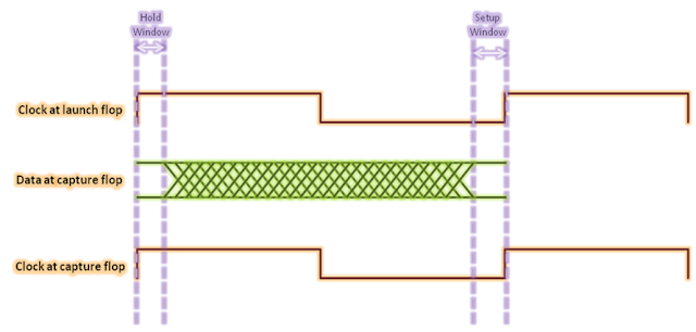
Data valid window for positive edge-trigger flop to positive edge-triggered flop path is equal to clock period minus sum of setup window and hold window requirements

Figure 3: Figure showing data valid window for rise-to-rise path

2)        Setup and hold checks for paths launching from positive edge-triggered flip-flop and being captured at negative edge-triggered flip-flop: In this case, both setup and hold check are half cycle checks; setup being checked on the next falling edge at the capture flop and hold on the previous falling edge of clock at the capture flop (data is launched at rising edge). Thus, with respect to (case 1) above, setup check has become tight and hold check has relaxed.


A timing path startgin from positive edge-triggered flop and ending at negative edge-triggered flop

Figure 4: Timing path from positive edge flop to negative edge flop (Rise-to-fall path)

Figure 5 below shows the setup and hold checks in the form of waveforms. As is shown, setup check occurs at the next falling edge and hold check occurs at the previous falling edge corresponding to the launch clock edge. The equation for setup check can be written, in this case, as:
            Tck->q + Tprop + Tsetup  < (Tperiod/2) + Tskew                       (for setup check)
And the equation for hold check can be written as:
            Tck->q + Tprop + (Tperiod/2) > Thold + Tskew                         (for hold check)
 

In case of path from positive edge-triggered flop to negative edge-triggered flop, setup check is on the next negative edge and hold check is on the previous falling edge corresponding to the edge at which data is launched (positive edge of the clock)

Figure 5: Setup and hold checks for rise-to-fall paths

Also, we show below the data valid and invalid windows. From this figure, 

                Data valid window = Clock period – Setup window – Hold window
                Start of data valid window = Tlaunch – (Tperiod/2)+ Thold
                End of data valid window = Tlaunch + (Tperiod/2) – Tsetup

As we can see, the data valid window is spread evenly on both sides of launch clock edge.

 
Data valid window in case of positive edge-triggered flop to negative edge-triggered flop path extends between the two negative edges, with setup and hold margins reduced from the corresponding sides

Figure 6: Figure showing data valid window for rise-to-fall path

3)           Setup and hold checks for paths launching from negative edge-triggered flip-flop and being captured at positive edge-triggered flip-flop (rise-to-fall paths): This case is similar to case 2; i.e. both setup and hold checks are half cycle checks. Data is launched on negative edge of the clock, setup is checked on the next rising edge and hold on previous rising edge of the clock.

Figure to show a timing path from a negative edge-triggered flip-flop to a positive edge-triggered flip-flop

Figure 7: Timing path from negative edge flop to positive edge flop (fall-to-rise path)

Figure 8 below shows the setup and hold checks in the form of waveforms. As is shown, setup check occurs at the next rising edge and hold check occurs at the previous rising edge corresponding to the launch clock edge.  The equation for setup check can be written, in this case, as:

            Tck->q + Tprop + Tsetup  < (Tperiod/2) + Tskew                       (for setup check)

And the equation for hold check can be written as:
            Tck->q + Tprop + (Tperiod/2) > Thold + Tskew                         (for hold check)

In case of timing path from negative edge-triggered flip-flop to positive edge-triggered flip-flop, data launches at the negative edge of the clock. The setup check is on the next positive edge and hold check is on the previous rising edge corresponding to the launching edge.

Figure 8: Setup and hold checks for fall to rise paths

Also, we show below the data valid and invalid windows. From this figure,

                Data valid window = Clock period – Setup window – Hold window
                Start of data valid window = Tlaunch – (Tperiod/2)+ Thold
                End of data valid window = Tlaunch + (Tperiod/2) – Tsetup

In this case too, data valid window spreads evenly on both the sides of launch clock edge.
 
Data valid window extends from the previous positive edge to next positive edge corresponding to launch edge, with setup and hold margind reduced from corresponding sides.

Figure 9: Figure showing data valid window for fall-to-rise path


4)             Setup and hold checks for paths launching from negative edge-triggered flip-flop and being captured at negative edge-triggered flip-flop (fall-to-fall paths): The interpretation of this case is similar to case 1. Both launch and capture of data happen at negative edge of the clock. Figure 10 shows a path being launched from a negative edge-triggered flop and being captured on a negative edge-triggered flop. In this case, setup check is on the next falling edge and hold check is on the same edge corresponding to the clock edge on which launching flop is launching the data.

Figure to show a timing path being launched from negatice edg of the clock and being captured at the negative edge of the clock

Figure 10: Path from negative edge flop to negative edge flop (fall to fall path)

Figure below shows the setup and hold checks in the form of waveforms. As is shown, setup check occurs at the next falling edge and hold check occurs at the same edge corresponding to the launch clock edge. 
The equation for setup check can be given as:
                Tck->q + Tprop + Tsetup < Tperiod + Tskew                (for setup check)
And the equation for hold check can be given as:
               Tck->q + Tprop > Thold + Tskew                                                    (for hold check) 


In case of paths starting from negative edge-triggered flop and ending at negative edge-triggered flop, data is launched from negative edge. Setup check is on the next negative edge and hold check is on the same edge corresponding to the launch clock edge

Figure 11: Setup and hold check for fall-to-fall path


Also, we show below the data valid and invalid windows. From this figure,

                Data valid window = Clock period – Setup window – Hold window
                Start of data valid window = Tlaunch + Thold
                End of data valid window = Tlaunch + Tperiod – Tsetup


Data valid window ranges between the two negative edges, with setup or hold margin reduced from each side

Figure 12: Figure showing data valid window for fall-to-fall path