A
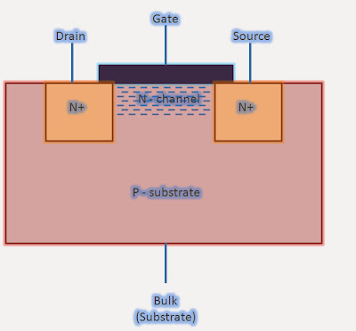
Metal Oxide Semiconductor Field Effect Transistors (MOSFET, or simply, MOS) is
a four terminal device. Figure 1 below shows the general representation of an
N-MOS (for PMOS, simply replace N regions with P and vice-versa). MOS is a
Voltage-controlled current source as the current through MOS is a function of
relative voltage levels of its terminals. The relative voltages of gate, drain
and source terminals (assuming bulk or substrate to be at same voltage as
source) determine the magnitude of current flowing in MOS. In each of these
regions, we can represent the current as a function of gate-to-source voltage
(VGS) and drain-to-source voltage (VDS).
 |
| MOS transistor - a 4-transistor device |
In a MOS device, the
current flows on formation of channel of carriers between source and drain
terminals. For this, voltage at gate terminal needs to be such that it attracts
carriers of appropriate type towards itself. When sufficient carriers are
attracted towards gate, channel is said to be formed. A current, then, flows
between source and drain terminals depending upon the voltage levels of these
terminals. The voltage level of substrate also impacts the magnitude of current
as it also determines the level of carriers in the channel.
For an N-MOS device, the
channel is formed by electrons. So, to attract electrons, gate voltage must be
greater than source voltage. For the formation of channel, the
difference between VG and VS (VG – VS)
must be greater than Vth (threshold voltage of the MOS).
Threshold voltage is
defined as the minimum difference in gate-to-source voltage needed for the
formation of channel in a MOS device. For NMOS, Vth is positive as
for channel formation gate needs to be at higher voltage as explained above. Similarly,
for PMOS, Vth is negative as gate needs to be at lower voltage than
source for channel to be formed.
On increasing gate voltage
beyond threshold voltage, current through MOS increases with increasing gate
voltage. Also, if we increase drain voltage keeping gate voltage constant,
current increases till a particular drain voltage. After that, increasing drain
voltage does not affect the current. Depending upon the relative voltages of
its terminals, MOS is said to operate in either of the cut-off, linear or
saturation region.
- Cut off region – A MOS device is said to be operating when the gate-to-source voltage is less than Vth. Thus, for MOS to be in cut-off region, the necessary condition is –
0 < VGS
< Vth - for NMOS
0 > VGS
> Vth - for
PMOS (as threshold voltage of PMOS is negative)
Cut-off region is also known as sub-threshold region. In this region, the dependence of current on gate voltage is exponential. The magnitude of current flowing through MOS in cut-off region is negligible as the channel is not present. The conduction happening in this region is known as sub-threshold conduction.
- Linear or non saturation region – For an NMOS, as gate voltage increases beyond threshold voltage, channel is formed between source and drain terminals. Now, if there is voltage difference between source and drain, current will flow. The magnitude of current increases linearly with increasing drain voltage till a particular drain voltage determined by the following relations –
VGS ≥
Vth
VDS < VGS
– Vth
The
current is, then, represented as a linear function of gate-to-source and
drain-to-source voltages. That is why, MOS is said to be operating in linear
region. The linear region voltage-current relation is given as follows:
Id(Linear) = µ Cox W/L
(Vgs – Vth – Vds/2) Vds.
Similarly, for P-MOS transistor, condition for P-MOS to be in linear region is represented as:
VGS < Vth
OR VSG > |Vth|
And VDS
> VGS + Vth OR VSD < VSG - |Vth|
- Saturation Region – For an NMOS, at a particular gate and source voltage, there is a particular level of voltage for drain, beyond which, increasing drain voltage seems to have no effect on current. When a MOS operates in this region, it is said to be in saturation. The condition is given as:
VGS
≥ Vth
VDS
> VGS – Vth
The current, now, is a function only
of gate and source voltages.
Id(saturation) = µ Cox
W/L (Vgs – Vth – Vds/2)2
Also read: