XNOR gate using NAND

As we know, the logical equation of a 2-input XNOR gate is given as below:
                      Y = A (xnor) B = (A' B '   +    A B)
Let us take an approach where we consider and A' as different variables for now (optimizations related to this, if any, will consider later). Thus, the logic equation, now, becomes:
                       Y = (CD    +    A B)           -----   (i)
     where
                      C = A'     and      D = B'
De-Morgan's law states that
                                m + n = (m'n')'

Taking this into account,
                     Y = ((CD)'(AB)')' = ((A' B')'  (A B)')'
Thus, Y is equal to ((A' nand B') nand (A nand B)). No further optimizations to the logic seem possible to this logic. Figure 1 below shows the implementation of XOR gate using 2-input NAND gates.
A 2 -input XOR gate implementation using NAND, XOR gate using NAND
Figure 1: 2-input XNOR gate implementation using NAND gates

2x1 mux using NAND gates

As we know, the logical equation of a 2-input mux is given as below:
                      Y = (s' A   +    s B)
Where s is the select of the multiplexer.
De-Morgan's law states that
                                m + n = (m'n')'

Taking this into account, here m = s'A  and  n = sB
                     Y = ((s'A)'(sB)')' = ((s' A)'  (s B)')'
Thus, Y is equal to ((s' nand A) nand (s nand B)). No further optimizations seem possible to this logic. Figure 1 below shows the implementation of 2:1 mux using 2-input NAND gates.
Figure 1: 2:1 Mux using NAND gates

3-input AND gate using 4:1 mux

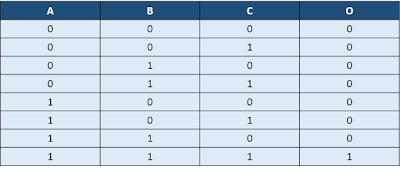
As we know, a AND gate's output goes '1' when all its inputs are '1', otherwise it is '0'. The truth table for a 3-input AND gate is shown below in figure 1, where A, B and C are the three inputs and O is the output.
                                      O = A (and) B (and) C
Truth table for 3-input AND gate


A 4:1 mux has 2 select lines. We can connect A and B to each of the select lines. The output will, then, be a function of the third input C. Now, if we sub-partition the truth table for distinct values of A and B, we observe
When A = 0 and B = 0, O = 0 => Connect D0 pin of mux to '0'
When A = 0 and B = 1, O = 0 => Connect D1 pin of mux to '0'
When A = 1 and B = 0, O = 0 => Connect D2 pin of mux to '0'
When A = 1 and B = 1, O = C => Connect D3 pin of mux to C
The implementation of 3-input AND gate, based upon our discussion so far, is as shown in figure 2 below:


Also read:

3-input XOR gate using 2-input XOR gates


A 3-input XOR gate can be implemented using 2-input XOR gates by cascading 2 2-input XOR gates. Two of the three inputs will feed one of the 2-input XOR gates. The output of the first gate will, then, be XORed with the third input to get the final output.

Let us say, we want to XOR three inputs A,B and C to get the output Z. First, XOR A and B together to obtain intermediate output Y. Then XOR Y and C to obtain Z. The schematic representation to obtain 3-input XOR gate by cascading 2-input XOR gates is shown in figure below:

Implementation of 3-input XOR gate using 2-input XOR gates


Clock gating interview questions

One of the most important and frequently asked topics in interviews is clock gating and clock gating checks. We have a collection of blog-posts related to this topic which can help you master clock gating. You can go through following links to add to your existing knowledge of clock gating:

  • Clock gating checksDiscusses different clock gating structures used and associated timing checks related to these
  • Clock gating checks at a muxDiscusses clock gating checks that should be applied in case one of the inputs of mux has a clock signal connected to it, which is the most common clock gating check in today's designs


Our purpose is to make this page a single destination for any questions related to clock gating. If you have any source of related and additional information, please comment or send an email to myblogvlsiuniverse@gmail.com and we will add it here. Also, feel free to ask any question related to clock gating.

Puzzles and brainteasers

A lot of questions in interviews are related to puzzles and brainteasers and are meant to relate to the thought process of the candidate. Listing below a few of the puzzles that may be of interest to you.

Please feel free to share puzzles that you think may be of interest to others. 

Why NAND structures are preferred over NOR ones?

Both NAND and NOR are classified as universal gates, but we see that NAND is preferred over NOR in CMOS logic structures. Let us discuss why it is so:


We know that when output is at logic 1, pull up structure for the output stage is on and it provides a path from VDD to output. Similarly, pull down structure provides a path from GND to output when output is logic 0. Pull up and pull down resistances are one of major factor in determining the speed of cell. The inverse of pull up and pull down resistances are called output high drive and output low drive of the cell respectively. In general, cells are designed to have similar drive strength of pull up and pull down structures to have comparable rise and fall time.


NMOS has half the resistance of an equal sized PMOS. let us say resistance of a given sized NMOS is R then resistance of  PMOS of same size will be 2R. In NAND gate, two NMOS are connected in series and two PMOS are connected in parallel. So, pull up and pull down resistances will be:

            Pull up resistance = 2R || 2R = R
            Pull down resistance = R + R = 2R


On the other hand, in a NOR gate, two NMOS are connected in parallel and two PMOS are connected in series. The pull-up and pull-down resistances, now, will be:

            Pull up resistance = 2R + 2R = 4R
            Pull down resistance = R || R = R/2


NAND gate has better ratio of output high drive and output low drive as compared to NOR gate. Hence NAND gate is preferred over NOR.


To use NOR gate as universal gate either pull up or pull down structure has to be resized(decrease the length of PMOS cells or increase length of NMOS cells) to have similar resistance as resistance is directly proportional to length (length of channel here).

Also read:

Divide by 2 clock in VHDL

Clock dividers are ubiquitous circuits used in every digital design. A divide-by-N divider produces a clock that is N times lesser frequency as compared to input clock. A flip-flop with its inverted output fed back to its input serves as a divide-by-2 circuit. Figure 1 shows the schematic representation for the same.

A divide by 2 clock circuit produces output clock that is half the frequency of the input clock
Divide by 2 clock circuit
                                          
Following is the code for a divide-by-2 circuit.
-- This module is for a basic divide by 2 in VHDL.
library ieee;
use ieee.std_logic_1164.all;
entity div2 is
                port (
                                reset : in std_logic;
                                clk_in : in std_logic;
                                clk_out : out std_logic
                );
end div2;

-- Architecture definition for divide by 2 circuit
architecture behavior of div2 is
signal clk_state : std_logic;
begin
                process (clk_in,reset)
                begin
                                if reset = '1' then
                                                clk_state <= '0';
                                elsif clk_in'event and clk_in = '1' then
                                                clk_state <= not clk_state;
                                end if;
                end process;
clk_out <= clk_state;

end architecture;

Hope you’ve found this post useful. Let us know what you think in the comments.

Applications of latches


A latch is a level-sensitive storage element capable of storing 1-bit digital data (Read more about basics of latches here). However simple that may sound, but there are countless applications in digital VLSI circuits as discussed below:
  • Master-slave flip-flop: Cascading of a positive latch and negative latch gives a negative edge-triggered flip-flop and cascading of negative and positve latch gives a positive edge-triggered flip-flop. This kind of design of edge-triggered flip-flops is the most prevalent architecture used in VLSI industry. In other words, all the flip-flops used in today's designs are actually two latches cascaded back-to-back.
Figure 1: Master-slave flip-flops using latches

  • Latch as lockup element: A latch is used as a savior for scan hold timing closure in the form of lockup latch. A lockup latch is nothing more than a transparent latch used in places where hold timing is an issue due to either very large clock skew or uncommon path, one of the commonoly occuring scenarios being scan connection between two functionally non-interacting domains. Read more about lockup latch
  • Latches used for permormance gain: Latches, due to their inherent property of time borrowing, can capture data over a period of time, rather than at a particular instant. This property of latch can be taken advantage of by the stage having maximum delay borrowing time from next stage; thus, reducing overall clock period. Read more here
  • Latch pipeline: Going one step further, there can be a whole design implemented with latches. The basic principle used is that a positive latch must be succeeded by a negative latch, and vice-versa. Using a latch based design, we can effectively get the job done at half the clock frequency. But, it is not feasible to fulfil the requirement of positive latch output going to negative latch. The effort required to build even a small latch based pipeline (even as small as that shown below in figure 2) is very latge. That is why, we never see practically latch pipeline based circuits.
Figure 2: Latch pipeline

  • Integrated Clock Gating Cell: Latch is used in the path of enable signal in case of clock gating elements in order to avoid glitches. An AND gate, in general, requires enable to launch from negative edge-triggered flip-flop and vice-versa. But it is very difficult to generalize a state-machine. Hence, latches are embedded alongside the AND gate (or OR gate) as a single standard cell to be used at places where clock gating is required. Read more here.
  • Latches in memory arrays to store data: Regenerative latches are used inside memory arrays of SRAM to store data. Regenerative latch, in general, forms part of a memory bit-cell. The number of such bit cells is equal to the number of bits that the memory can store.
So, we have gone through a few of the applications of latches. Can you think of any other application of latches in designs? Please do not hesitate to share your knowledge with others. :-)

Some Interesting lInux commands Usage

Write a linux command that prints the list of all the unique include files in all the c++ files in a given area : 

Answer :

         find . -name "*.cxx" | xargs grep "#include" | awk '{print $2}' | sort -u

Clock gating - basics

The dynamic power associated with any circuit is related to the amount of switching activity and the total capacitive load. In digital VLSI designs, the most frequently switching element are clock elements (buffers and other gates used to transport clock signal to all the synchronous elements in the design). In some of the designs, clock switching power may be contributing as high as 50% of the total power. Power being a very critical aspect, we need to make efforts to reduce this. Any effort that can be made to save the clock elements toggling can help in reducing the total power by a significant amount. Clock gating is one of the techniques used to save the dynamic power of clock elements in the design.

Principle behind clock gating: The principle behind clock gating is to stop the clock of those sequential elements whose data is not toggling. RTL level code talks only about data transfer. It may have some condition wherein a flip-flop will not toggle its output if that condition is met. Figure 1 below shows such a condition. In it, FF1's output will remain stable as long as EN = 0. On the right hand side, its equivalent circuit is provided, wherein EN has been translated into an AND gate in the clock path.This is a very simplistic version of what modern-day synthesis tools do to implement clock gating.

Figure 1: Clock gating implementation
Implications of clock gating: The implementation of clock gating, as expected, is not so simple. There are multiple things to be taken into account, some of which are:
  • Timing of enable (EN) signal: The gating of clock can cause a glitch in clock, if not taken care of by architectural implementation. Clock gating checks discusses what all needs to be taken care of as regards timing in clock gating implementation.
Area/power/latency trade-off: As is shown in figure 1, clock gating transfers a data-path logic into clock path. This can increase overall clock latency. Also, area penalty can be there, if the area of clock gating structure is more. Power can also increase, instead of decreasing, if only 1-2 flops' structure is replaced by clock gating (depending upon the switching power of clock gating structure vs those inside flip-flop). Normally, a bunch of flops with similar EN condition are chosen, and a common clock gating is inserted for those, thereby minimizing area and power penalties.

Also read:

Setup time

Definition of setup time: Setup time is defined as the minimum amount of time before arrival of clock's active edge so that it can be latched properly. In other words, each flip-flop (or any sequential element, in general) needs data to be stable for some time before arrival of clock edge such that it can reliably capture the data. This amount of time is known as setup time.

We can also link setup time with state transitions. We know that the data to be captured at the current clock edge was launched at previous clock edge by some other flip-flop. The data launched at previous clock edge must be stable  at least setup time before the current clock edge. So, adherence to setup time ensures that the data launched at previous edge is captured at the current clock edge reliably. In other words, setup time ensures that the design transitions to next state smoothly.

Figure 1: Setup time

Figure 1 shows that data is allowed to toggle prior to yellow dotted line. This yellow dotted line corresponds to setup time. The time difference between this line and active clock edge is termed as setup time. Data cannot toggle after this yellow dotted line for a duration known as setup-hold window. Occurrence of such an event will be termed as setup time violation. The consequence of setup time violation can be capture of wrong data or the sequential element (setup check violation) going into metastable state (setup time violation).


Figure 2: A positive level-sensitive D-latch
Latch setup time: Figure 2 shows a positive level-sensitive latch. If there is a toggling of data at the latch input close to negative edge (while the latch is closing), there will be an uncertainty as if data will be capture reliably or not. For data to be captured reliably, it has to be available at the input of loop transmission gate at the arrival of closing clock edge. To be able to present at NodeD at the closing edge, it must be there at latch input some time prior to the clock edge. This time in reaching from latch input to NodeD is termed as setup time for this latch.

Flip-flop setup time: Figure 3 below shows a master-slave negative edge-triggered D flip-flop using transmission gate latches. This is the most popular configuration of a flip-flop used in today's designs. Let us get into the details of setup time for this flip-flop. For this flip-flop to capture data reliably, the data must be present at nodeF at the arrival of negative edge of clock. So, data must travel NodeA -> NodeB -> NodeC -> NodeD -> NodeE -> NodeF before clock edge arrives. To reach NodeF at the closing edge of latch1, data should be present at NodeA at some earlier time. This time taken by data to reach NodeF is the setup time for flip-flop under consideration (assuming CLK and CLK' are present instantaneously. If that is not the case, it will be accounted for accordingly). We can also say that the setup time of flip-flop is, in a way, setup time of master latch.
 A D-type flip-flop consists of two latches connected back to back in master-slave format
Figure 3: D-flip flop