Today’s designs are dominated by digital devices. These are
all synchronous state machines consisting of flip-flops. The transition from
one state to next is synchronous and is governed by a signal known as clock. That is why, we have aptly
termed clock as ‘the in-charge of
synchronous designs’.
Definition of clock signal: We can define a clock signal as the one which synchronizes the state transitions by keeping all the registers/state elements in synchronization. In common terminology, a clock signal is a signal that is used to trigger sequential devices (flip-flops in general). By this, we mean that ‘on the active state/edge of clock, data at input of flip-flops propagates to the output’. This propagation is termed as state transition. As shown in figure 1, the ‘2-bit’ ring counter transitions from state ‘01’ to ‘10’ on active clock edge.
 |
|
Figure
1: Figure showing state
transition on active edge of clock
|
Clock signals occupy a very important place throughout the
chip design stages. Since, the state transition happens on clock transition,
the entire simulations including verification, static timing analysis and gate
level simulations roam around these clock signals only. If Static timing
analysis can be considered as a body, then clock is its blood. Also, during
physical implementation of the design, special care has to be given to the
placement and routing of clock elements, otherwise the design is likely to
fail. Clock elements are responsible for almost half the dynamic power
consumption in the design. That is why; clock has to be given the prime
importance.
Clock tree:
A clock signal originates from a clock source. There may be designs with a
single clock source, while some designs have multiple clock sources. The clock
signal is distributed in the design in the form of a tree; leafs of the tree
being analogous to the sequential devices being triggered by the clock signal
and the root being analogous to the clock source. That is why; the distribution
of clock in the design is termed as clock
tree. Normally, (except for sometimes when intentional skew is introduced
to cater some timing critical paths), the
clock tree is designed in such a way that it is balanced. By balanced clock
tree, we mean that the clock signal reaches each and every element of the
design almost at the same time. Clock
tree synthesis (placing and routing clock tree elements) is an important
step in the implementation process. Special cells and routing techniques are
used to ensure a robust clock tree.
Clock domains: By
clock domain, we mean ‘the set of flops being driven by the clock signal’. For
instance, the flops driven by system clock constitute system domain. Similarly,
there may be other domains. There may be multiple clock domains in a design;
some of these may be interacting with each other. For interacting clock
domains, there must be some phase relationship between the clock signals
otherwise there is chance of failure due to metastability. If phase relationship is
not possible to achieve, there should be clock domain synchronizers to reduce
the probability of metastability failure.
Specifying a signal
as clock: In EDA tools, ‘create_clock’
command is used to specify a signal as a clock. We have to pass the period of
the clock, clock definition point, its reference clock (if it is a generated
clock as discussed below), duty cycle, waveform etc. as argument to the
command.
Master and generated clocks: EDA tools have the concept of master and generated clocks. A generated clock is the one that is derived from another clock, known as its master clock. The generated clock may be of the same frequency or different frequency than its master clock. In general, a generated clock is defined so as to distinguish it from its master in terms of frequency, phase or domain relationship.
Some terminology
related to clock: There are different terms related to clock signals,
described below:
- Leading and trailing clock edge: When clock signal transitions from ‘0’ to ‘1’, the clock edge is termed as leading edge. Similarly, when clock signal transitions from ‘1’ to ‘0’, the clock edge is termed as trailing edge.
 |
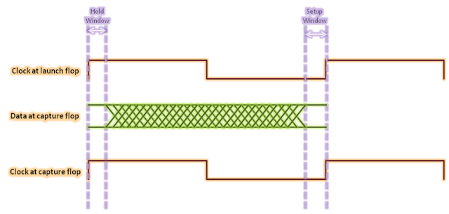
- Launch and capture edge: Launch edge is that edge of the clock at which data is launched by a flop. Similarly, capture edge is that edge of the clock at which data is capture by a flop.
- Clock skew: Clock skew is defined as the difference in arrival times of clock signals at different leaf pins. Considering a set of flops, skew is the difference in the minimum and maximum arrival times of the clock signal. Global skew is the clock skew for the whole design. On the contrary, considering only a portion of the design, the skew is termed as local skew.


