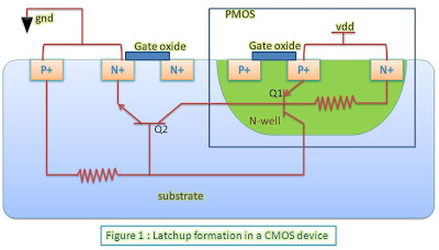
What is Latchup: Latchup refers to short circuit formed between power and ground rails in
an IC leading to high current and damage to the IC. Speaking about CMOS
transistors, latch up is the phenomenon of low impedance path between
power rail and ground rail due to interaction between parasitic pnp and npn
transistors. The structure formed by these resembles a Silicon Controlled rectifier (SCR, usually known as a thyristor, a PNPN device used in power
electronics). These form a +ve feedback loop, short circuit the power rail and
ground rail, which eventually causes excessive current, and can even permanently damage
the device.
 |
| Figure 1: Latchup formation in CMOS |
Analysis of latchup formation: Unless SCR is triggered by an external disturbance, the
collector current of both transistors consists of reverse leakage current. But if
collector current of one of BJT is temporarily increased by disturbance,
resulting positive feedback loop causes current perturbation to be multiplied
by β1β2 as explained below. The disturbance may be a spike of input voltage on
an input or output pin, leading to junction breakdown, or ionizing radiations.
Because collector current of one transistor Q1 is fed as
input base current to another transistor Q2, collector current of Q2, Ic2 =
β2 * Ib2 and this collector current Ic2 is fed as input base current
Ib1 to another transistor Q1. In this way both transistors feedback
each other and the collector current of each goes on multiplying.
Net gain of SCR device = β1 *β2
Total current in one loop = current perturbation * Gain
If β1 *β2 >=1, both
transistors will conduct a high saturation current even after the triggering
perturbation is no longer available. This current will eventually becomes so
large that it may damage the device.
Latch-up prevention techniques: Simply put, latchup prevention/protection includes putting a high resistance in the path so as to limit the current
through supply and make β1 *β2 < 1. This can be done with the help of following techniques:
- Surrounding PMOS and NMOS transistors with an insulating oxide layer (trench). This breaks parasitic SCR structure.
- Latchup Protection Technology circuitry which shuts off the device when latchup is detected.