Showing posts with label on chip variations. Show all posts

On-chip variations – the STA takeaway

Static timing analysis of a design is performed to estimate its working frequency after the design has been fabricated. Nominal delays of the logic gates as per characterization are calculated and some pessimism is applied above that to see if there will be any setup and/or hold violation at the target frequency. However, all the transistors manufactured are not alike. Also, not all the transistors receive the same voltage and are at same temperature.  The characterized delay is just the delay of which there is maximum probability. The delay variation of a typical sample of transistors on silicon follows the curve as shown in figure 1. As is shown, most of the transistors have nominal characteristics. Typically, timing signoff is carried out with some margin. By doing this, the designer is trying to ensure that more number of transistors are covered. There is direct relationship between the margin and yield. Greater the margin taken, larger is the yield. However, after a certain point, there is not much increase in yield by increasing margins. In that case, it adds more cost to the designer than it saves by increase in yield. Therefore, margins should be applied so as to give maximum profits.

Most of the transisors have close to nominal delay. However, some transistors have delay variations. Theoretically, there is no bound existing for delay variations. However, probabilty of having that delay decreases as delay gets far from nominal.
Number of transistors v/s delay for a typical silicon transistors sample


We have discussed above how variations in characteristics of transistors are taken care of in STA. These variations in transistors’ characteristics as fabricated on silicon are known as OCV (On-Chip Variations). The reason for OCV, as discussed above also, is that all transistors on-chip are not alike in geometry, in their surroundings, and position with respect to power supply. The variations are mainly caused by three factors:
  • Process variations: The process of fabrication includes diffusion, drawing out of metal wires, gate drawing etc. The diffusion density is not uniform throughout wafer. Also, the width of metal wire is not constant. Let us say, the width is 1um +- 20 nm. So, the metal delays are bound to be within a range rather than a single value. Similarly, diffusion regions for all transistors will not have exactly same diffusion concentrations. So, all transistors are expected to have somewhat different characteristics.
  • Voltage variation: Power is distributed to all transistors on the chip with the help of a power grid. The power grid has its own resistance and capacitance. So, there is voltage drop along the power grid. Those transistors situated close to power source (or those having lesser resistive paths from power source) receive larger voltage as compared to other transistors. That is why, there is variation seen across transistors for delay.
  • Temperature variation: Similarly, all the transistors on the same chip cannot have same temperature. So, there are variations in characteristics due to variation in temperatures across the chip.


How to take care of OCV: To tackle OCV, the STA for the design is closed with some margins. There are various margining methodologies available. One of these is applying a flat margin over whole design. However, this is over pessimistic since some cells may be more prone to variations than others. Another approach is applying cell based margins based on silicon data as what cells are more prone to variations. There also exist methodologies based on different theories e.g. location based margins and statistically calculated margins. As advances are happening in STA, more accurate and faster discoveries are coming into existence.

Lockup latch – principle, application and timing

What are lock-up latches: Lock-up latch is an important element in scan-based designs, especially for hold timing closure of shift modes. Lock-up latches are necessary to avoid skew problems during shift phase of scan-based testing. A lock-up latch is nothing more than a transparent latch used intelligently in the places where clock skew is very large and meeting hold timing is a challenge due to large uncommon clock path. That is why, lockup latches are used to connect two flops in scan chain having excessive clock skews/uncommon clock paths as the probability of hold failure is high in such cases. For instances, the launching and capturing flops may belong to two different domains (as shown in figure below). Functionally, they might not be interacting. Hence, the clock of these two domains will not be balanced and will have large uncommon path. But in scan-shift mode, these interact shifting the data in and out. Had there been no lockup latches, it would have been very difficult for STA engineer to close timing in a scan chain across domains. Also, probability of chip failure would have been high as there a large uncommon path between the clocks of the two flops leading to large on-chip-variations. That is why; lockup latches can be referred as as the soul mate of scan-based designs.

Lockup latches are needed where there is need to fix hold due to large skew between clock signals for launch and capture flops

Figure 1 : Lockup latches - the soul mate of scan-based designs


Where to use a lock-up latch: As mentioned above, a lock-up latch is used where there is high probability of hold failure in scan-shift modes. So, possible scenarios where lockup latches are to be inserted are:

  • Scan chains from different clock domains: In this case, since, the two domains do not interact functionally, so both the clock skew and uncommon clock path will be large.
  • Flops within same domain, but at remote places: Flops within a scan chain which are at remote places are likely to have more uncommon clock path. 
In both the above mentioned cases, there is a great chance that the skew between the launch and capture clocks will be high. There is both the probability of launch and capture clocks having greater latency. If the capture clock has greater latency than launch clock, then the hold check will be as shown in timing diagram in figure 3. If the skew difference is large, it will be a tough task to meet the hold timing without lockup latches.

A timing path crossing from one domain to another

Figure 2: A path crossing from domain 1 to domain 2 (scope for a lock-up latch insertion)

Waveform showing the skew between launch and capture clocks, resulting in hold violation

Figure 3: Timing diagram showing setup and hold checks for path crossing from domain 1 to domain 2

Positive or negative level latch?? It depends on the path you are inserting a lock-up latch. Since, lock-up latches are inserted for hold timing; these are not needed where the path starts at a positive edge-triggered flop and ends at a negative edge-triggered flop. It is to be noted that you will never find scan paths originating at positive edge-triggered flop and ending at negative edge-triggered flop due to DFT specific reasons. Similarly, these are not needed where path starts at a negative edge-triggered flop and ends at a positive edge-triggered flop. For rest two kinds of flop-to-flop paths, lockup latches are required. The polarity of the lockup latch needs to be such that it remains open during the inactive phase of the clock. Hence,

  • For flops triggering on positive edge of the clock, you need to have latch transparent when clock is low (negative level-sensitive lockup latch)
  • For flops triggering on negative edge of the clock, you need to have latch transparent when clock is high (positive level-sensitive lockup latch)
Who inserts a lock-up latch: These days, tools exist that automatically add lockup latches where a scan chain is crossing domains. However, for cases where a lockup latch is to be inserted in an intra-domain scan chain (i.e. for flops having uncommon path), it has to be inserted during physical implementation itself as physical information is not feasible during scan chain implementation (scan chain implementation is carried out at the synthesis stage itself).

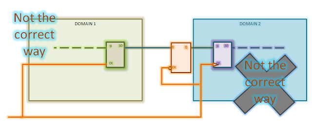
Which clock should be connected to lock-up latch: There are two possible ways in which we can connect the clock pin of the lockup latch inserted. It can either have same clock as launching flop or capturing flop. Connecting the clock pin of lockup latch to clock of capturing flop will not solve the problem as discussed below.
  •  Lock-up latch and capturing flop having the same clock (Will not solve the problem): In this case, the setup and hold checks will be as shown in figure 5. As is apparent from the waveforms, the hold check between domain1 flop and lockup latch is still the same as it was between domain 1 flop and domain 2 flop before. So, this is not the correct way to insert lockup latch.


It is not appropriate to connect the capture flop's clock to the lockup latch as hold check will be the same

Figure 4: Lock-up latch clock pin connected to clock of capturing flop

Waveform showing the inability of connecting capture flop's clock in meeting hold

Figure 5: Timing diagrams for figure 4


  •  Lock-up latch and launching flop having the same clock: As shown in figure 7, connecting the lockup latch to launch flop’s clock causes the skew to reduce between the domain1 flop and lockup latch. This hold check can be easily met as both skew and uncommon clock path is low. The hold check between lockup latch and domain2 flop is already relaxed as it is half cycle check. So, we can say that the correct way to insert a lockup latch is to insert it closer to launching flop and connect the launch domain clock to its clock pin.

The correct way to connect the clock to lockup latch is to connect it with the clock coming at launch flop

Figure 6: Lock-up latch clock pin connected to clock of launch flop

Waveform for the connection of clock pin of lockup latch to launch flop's clock

Figure 7: Waveforms for figure 6


Why don’t we add buffers: If the clock skew is large at places, it will take a number of buffers to meet hold requirement. In normal scenario, the number of buffers will become so large that it will become a concern for power and area. Also, since skew/uncommon clock path is large, the variation due to OCV will be high. So, it is recommended to have a bigger margin for hold while signing it off for timing. Lock-up latch provides an area and power efficient solution for what a number of buffers together will not be able to achieve.

Advantages of inserting lockup latches:
  • Inserting lock-up latches helps in easier hold timing closure for scan-shift mode
  • Robust method of hold timing closure where uncommon path is high between launch and capture flops
  • Power efficient and area efficient
  • It improves yield as it enables the device to handle more variations.
Lockup registers: Instead of latches, registers can also be used as lockup elements; however, they have their own advantages and disadvantages. Please refer to Lockup latches vs. lockup registers : what to chose for a comparative study of using lockup latches vs lockup registers.

References:
1)  Why not add buffer but lockup latch” - http://www.edaboard.com/thread82364.html

Also read: