Showing posts with label Metastablity. Show all posts

Minimum pulse width

All the sequential elements need some minimum pulse (either high or low) to ensure that the data has been captured correctly. In other words, clock pulse fed to a flop or latch (or any other sequential element) must be wide enough so that it does not interfere with correct functionality of the element. By correct functionality, is meant, the internal operations of the cell.

Minimum pulse width requirement: To understand minimum pulse width requirement, let us first define pulse width. Formally, pulse width can be defined as:

"If talking in terms of high signal level (high minimum pulse width), it is the time interval between clock signal crossing half the VDD level during rising edge of clock signal and clock signal crossing half the VDD level during falling edge of clock signal. If talking in terms of low signal level (low minimum pulse width), it is the time interval between clock signal crossing half the VDD level during falling edge of the clock signal and clock signal crossing half the VDD level during rising edge of the clock signal."

If the clock being fed to a sequential object has less pulse width than the minimum required, either of the following is the probable output:
  • The flop can capture the correct data and FSM will functional correctly
  • The flop can completely miss the clock pulse and does not capture any new data. The FSM will, then, lead to invalid state
  • The flop can go meta-stable
All these scenarios are probable of happening; so, it is required to ensure every sequential element always gets a clock pulse greater than minimum pulse width required. To ensure this, there are ways to communicate to timing analysis tool the minimum pulse width requirement for each and every sequential element. The check to ensure minimum pulse width is known as "minimum pulse width check". There are following ways to ensure minimum pulse width through minimum pulse width check:


  • Through liberty file: By default, all the registers in a design should have a minimum pulse width defined through liberty file as this is the format to convey the standard cell requierements to STA tool. By convention, minimum pulse width should be defined for clock and reset pins. Minimum pulse width is constrained in liberty file using following syntax:
                                        Timing type : min_pulse_width;
  • Through SDC command: We can also define minimum pulse width requirement through SDC command. The SDC command for the same is "set_min_pulse_width". For example, following set of commands will constrain the minimum pulse width of clock clk to be 5 ns high and 4 ns low:
                               set_min_pulse_width -high 5 [get_clocks clk]
                               set_min_pulse_width -low  4 [get_clocks clk]

Can hold check be frequency dependant?


We often encounter people argue that hold check is frequency independent. However, it is only partially true. This condition is true only for zero-cycle hold checks. By zero cycle hold checks, we mean that the hold check is performed on the same edge at which it is launched. This is true in case of timing paths between same polarity registers; e.g. between positive edge-triggered flops. Figure 1 below shows timing checks for a data-path launched from a positive edge-triggered flip-flop and captured at a positive edge-triggered flip-flop. The hold timing, in this case, is checked at the same edge at which data is launched. Changing the clock frequency will not cause hold check to change.

Setup check for positive edge-triggered flip-flop to positive edge-triggered flip-flop is single cycle and hold check is zero cycle
Figure 1: Setup and hold checks for positive edge-triggered to positive edge-triggered flip-flop
Most of the cases in today’s designs are of this type only. The exceptions to zero cycle hold check are not too many. There are hold checks for previous edge also. However, these are very relaxed as compared to zero cycle hold check. Hence, are not mentioned. Also, hold checks on next edge are impossible to be met considering cross-corner delay variations. So, seldom do we hear that hold check is frequency dependant. Let us talk of different scenarios of frequency dependant hold checks:

  1.  From positive edge-triggered flip-flop to negative edge-triggered flip-flop and vice-versa: Figure 2 below shows the setup and hold checks for a timing path from positive edge-triggered flip-flop to a negative edge-triggered flip-flop. Change in frequency will change the distance between the two adjacent edges; hence, hold check will change. The equation for hold timing will be given for below case as:

Tdata + Tclk/2 > Tskew + Thold
or
Tslack =  Tclk/2 - Thold - Tskew + Tdata
          Thus, clock period comes into picture in calculation of hold timing slack.

Both setup and hold checks are half cycle. Setup is checked on next edge whereas hold is checked on previous edge
Figure 2: Setup and hold checks for timing path from positive edge-triggered flip-flop to negative edge-triggered flip-flop

Similarly, for timing paths launching from negative edge-triggered flip-flop and being captured at positive edge-triggered flip-flop, clock period comes into picture. However, this check is very relaxed most of the times. It is evident from above equation that for hold slack to be negative, the skew between launch and capture clocks should be greater than half clock cycle which is very rare scenario to occur. Even at 2 GHz frequency (Tclk = 500 ps), skew has to be greater than 250 ps which is still very rare.
Coming to latches, hold check from a positive level-sensitive latch to negative edge-triggered flip-flop is half cycle. Similarly, hold check from a negative level-sensitive latch to positive edge-triggered flip-flop is half cycle. Hence, hold check in both of these cases is frequency dependant.

2. Clock gating hold checks: When data launched from a negative edge-triggered flip-flop gates a clock on an OR gate, hold is checked on next positive edge to the edge at which data is launched as shown in figure 3, which is frequency dependant.

Setup check is single cycle and hold check is half cycle and checked on next clock edge with respect to launch clock edge
Figure 3: Clock gating hold check between data launched from a negative edge-triggered flip-flop and and clock at an OR gate

           Similarly, data launched from positive edge-triggered and gating clock on an AND gate form half cycle hold. However, this kind of check is not possible to meet under normal scenarios considering cross-corner variations.

3)      Non-default hold checks: Sometimes, due to architectural requirements (e.g. multi-cycle paths for hold), hold check is non-zero cycle even for positive edge-triggered to positive edge-triggered paths as shown in figure 4 below.
Figure 4: Non-default hold check with multi-cycle path of 1 cycle specified


Race condition in digital circuits


In general, race condition refers to a situation in which the result depends upon the sequence in which events happen. In particular, a race condition occurs when a system/device is designed assuming a particular sequence of events without taking steps to ensure it. In logic gates, it happens when the inputs arrive at the gate in a sequence not assumed while deriving the function. This results, sometimes, in the anomalous behavior of the logic gate because of the unexpected dependence on the sequence of arrival of inputs. Since, the function of the logic gate is calculated assuming static inputs; the order of arrival may have impact on the output. We can consider race condition as a situation in which two or more signals are racing to have their effect on the output. This is how; race condition derives its name.
For a very simple example, consider the following logic function-
Z = A . A’

AND gate having race condition
Figure 1: An example digital circuit having race condition


Theoretically, the output will always be ‘0’. However, this is true only if the non-inverted portion of the signal has greater delay in reaching the AND gate (we have considered ‘0’ -> ‘1’ transition of the input signal ‘A’). As shown in the figure above, the signal passing through inverter will have some delay of its own. If the signal through inverter reaches the AND gate later than the one without inverter, there will be a glitch as shown in the figure 2. For ‘1’ -> ‘0’ transition, the opposite will happen.

The above circuit requires a certain relationship between arrival times of the two signals. If the relationship is not ensured, glith will be caused.
Figure 2: Glitch caused at the output of AND gate due to inverted signal being delayed than non-inverted signal


What can be the consequences: If the condition for race is violated, the design may enter an undefined state, the one which might not have been considered while designing. Hence, the whole system will malfunction in such a scenario leading to failure. It might be the case that some elements in the design enter metastable state, which can further cause problems. Hence, it is very important to give proper consideration to race conditions.
How can we prevent race condition: Normally, in digital designs, as long as setup and hold checks are met for each flip-flop, we do not need to worry about the race conditions in the design under consideration. But, there are some conditions like the output of the above AND gate might be used as a clock for some flop. In that case, we need to consider the race condition. We need to have proper sequencing of signals so as to have the desired output. Had the above case been in reality, it might be wise to delay the non-inverted signal. Race conditions in the design can be eliminated by using proper design techniques (e.g. K-map). Using these, designers and recognize and eliminate the race conditions before they cause problems.

Read also:

Metastability


What is metastability: Metastability is a phenomenon of unstable equilibrium in digital electronics in which the sequential element is not able to resolve the state of the input signal; hence, the output goes into unresolved state for an unbounded interval of time. Almost always, this happens when data transitions very close to active edge of the clock, hence, violating setup and hold requirements. Since, data makes transition close to active edge of clock, the flop is not able to capture the data completely. The flop starts to capture the data and output also starts to transition. But, before output has changed its state, the input is cut-off from the output as clock edge has arrived. The output is, then, left hanging between state ‘0’ and state ‘1’. Theoretically, the output may remain in this state for an indefinite period of time. But, given the time to settle down, the output will eventually settle to either its previous state or the new state. Thus, the effect of signal present at input of flop may not travel to the output of the flop partly or completely. In other words, we can say that when a flip-flop enters metastable state, one cannot predict its output voltage level after it exits the metastability state nor when the output will settle to some stable voltage level. The metastability failure is said to have occurred if the output has not resolved itself by the time it must be available for use. Also, since, the output remains in-between ‘0’ and ‘1’, which means both P-MOS and N-MOS are not switched off. Hence, VDD is shorted to GND terminal making it cause a high current to flow through as long as the output is hanging in-between.


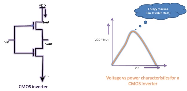
Metastability example: Consider a CMOS inverter circuit as shown below. The current vs voltage (we can also say power vs voltage as VDD is constant) characteristics for this circuit are also shown. It can be observed that output current is 0 for both input voltage levels; i.e. ‘0’ and ‘1’. As the voltage level is increased from ‘logic 0’, the current increases. It attains its maximum value at ‘Vin’ somewhere near VDD/2. It again starts decreasing as ‘Vin’ is increased further and again becomes 0 when ‘Vin’ is at ‘logic 1’. Thus, there is a local maxima for power consumption for CMOS inverter. At this point, the device is in unstable equilibrium. As for CMOS inverter, for other CMOS devices too, there lies ‘a local maxima’ at some value of input voltage. We all know that for a flip-flop, the output stage is a combinational gate (mostly an inverter). So, we can say that the output of the flip-flop is prone to metastability provided right input level.


Power characteristics of CMOS inverter
Figure 1: Power characteristics of CMOS inverter

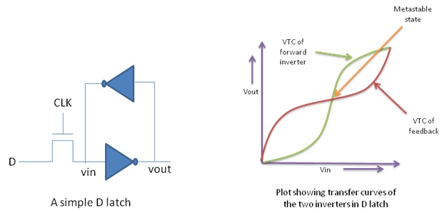
As we now know that a CMOS combinational gate has a point on its ‘voltage characteristic’ curve that is quasi-stable, let us look at a CMOS latch from the same perspective. The CMOS latch has a transmission gate followed by two inverters connected in feedback loop. The voltage characteristic curves for the two inverters are shown. The metastable point, here, lies where the two curves intersect as this point is the resulting peak point of the ‘Superposition curve’ resulting from the two individual curves. A latch goes into metastable state very frequently, especially if the input is changing fast. But, this metastability is resolved quickly as the output tends to go to one of its stable states. As a flop is generally made by connecting two latches in master-slave configuration, the flops are also prone to be metastable. The difference here is just that the probability of a flip-flop being metastable is a lot less than latches as ‘flops are edge sensitive’ as compared to latches which are level sensitive.


Figure showing transfer curve for D-latch and metastable point
Figure 2: Transfer curves of two inverters in a D-latch


We have just came to know that different elements are prone to metastability to different extents. There is a measure to determine the extent to which an element is prone to metastability failure. This is given by an interval known as ‘Mean Time Between Failures’ (MTBF) and is a measure of how prone an element is to failure. It gives the average time interval between two successive failures. The failure rate is given as the reciprocal of MTBF.