Showing posts with label VLSI. Show all posts

Noise margins


In this realistic world, nothing is ideal. A signal travelling along a wire/cable/transmission line is susceptible to noise from the surroundings. Also, there is degradation in signal due to parasitic elements involved in the line. Moreover, the output signal produced by the transmitter itself only does resemble the ideal signal thereby worsening the scenario. There are repeaters/buffers along the line to minimize the impact of noise. But there is a limit up to which degradation is allowed beyond which the receiver is unable to sense the correct value of the signal. This degradation is measured in terms of noise margins. One can find the topic discussed in all the textbooks related to digital logic and system design might it be CMOS, TTL or any other logic family.

Let us illustrate the concept of noise margins with the help of an example. Let us assume that a signal has to travel from a transmitter to a receiver through an inter-connect element (or, commonly called as a net) which will only degrade the signal, since there is no active element in-between transmitter and receiver. The output signal produced by Transmitter (Tx) will deviate from ideal voltage levels as is shown in figures 1 and 2 for logic level ‘1’. In addition, there will be signal degradation by inter-connect element as well as noise induced from the surroundings. As a result, the band of voltages that can be present at the receiver input for logic ‘1’ will further widen. Now, there are two cases:

  1. If the band voltages recognized as logic ‘1’ by the receiver is super-set of the band of voltages that can exist at the receiver input as shown in figure 1, receiver will recognize the transmitted logic ‘1’ for all the cases. This is the desired scenario as no logic ‘1’ transmitted will be missed by the receiver. This scenario is depicted in figure 1, wherein the noise induced by surroundings is such that the range of voltages present at the receiver does not violate the band of voltages recognized as voltage '1' by the receiver. So, it will be recognized correctly as logic '1' by the receiver.

When the noise induced is less than noise margin, it will be captured properly by the receiver
Figure 1: Figure showing the noise induced is less than noise margin


2)  If the band of values recognized as logic ‘1’ by the receiver is a sub-set of the band of voltages that can exist at the receiver input as shown in figure 2, there will be some cases that will not be recognized as logic ‘1’, but are intended to be recognized. So, there will be a loss of information/incorrect transmission of information possible in such cases. This scenario is depicted in figure 2, wherein the noise induced by surroundings makes the band of voltage at the receiver's input larger than that can be decoded correctly as logic '1' by the receiver. So, there is no guarantee that the signal will be perceived as logic '1' by the receiver.

Figure showing the noise induced is less than noise margin. In case this happens, the signal will not be correctly decoded by the receiver.
Figure 2: Figure showing the noise induced is greater than noise margin
Let us now label each of these regions to make the discussion more meaningful. The lowest voltage that will be produced as logic ‘1’ by the transmitter is termed as VOH and, let us say, highest is VDD. (We are here considered about lower level only). So, the range of voltages produced by the transmitter is (VDD – VOH).  And let the receiver accept voltages higher than VIH. So the range of voltages accepted by the receiver will be (VDD – VIH). So, the maximum degradation that can happen over the communication channel is (VOH – VIH) which is nothing but the noise margin. If the degradation is less than this figure, the logic ‘1’ will be recognized correctly by the receiver; otherwise it won’t. So, the noise margin equation can be given as below for logic '1':


Noise margin for logic '1' (NM) = VOH – VIH
Where
VOH = Lowest level of voltage that can be produced as logic '1' by the transmitter
VIH = Lowest level of voltage that can be recognized as logic '1' by the receiver

Similarly, for logic ‘0’, the range of outputs that can be produced by the transmitter is (0 - VOL) and the range of input voltages that can be detected by the receiver is (0 – VIL), thereby providing the noise margin as:
Noise margin (NM) = VIL – VOL

Where

VIL = Highest level of voltage that can be recognized as logic ‘0’ by the receiver.
VIH = Highest level of voltage that is produced as logic ‘0’ by the transmitter.

Figure 3 shows all these levels for the example we had taken earlier to demonstrate the concept of noise margins.

Noise margin calculation.
Figure 3: Noise margin

From out preceding discussion, if the degradation over the communication channel is more than noise margin, it will not be detected correctly by the receiver. So, it is imperative for the designer to design accordingly.


Definition of noise margin: Thus, we can conclude this post by defining noise margin as below:
"Noise margin is the difference between the worst signal voltage produced by the transmitter and the worst signal that can be detected by receiver."
Also read

Technology scaling factor

Technology nodex always shrinks by a factor of 0.7 per generation so that each subsequent technology has cell area that is half of that in present technology node.
For instance, you will find technology nodes as 180 um 90 um, 65 um, 45 um, 32 um, 22 um and so on..
*Source - Digital integrated circuits - A design perspective by Jan M Rabay

Can a net have negative propagation delay?


As we discussed in ‘’Is it possible for a logic gate to have negative propagation delay”, a logic cell can have negative propagation delay. However, the only condition we mentioned was that the transition at the output pin should be improved drastically so that 50% level at output is reached before 50% level of input waveform.

In other words, the only condition for negative delay is to have improvement in slew. As we know, a net has only passive parasitic in the form of parasitic resistances and capacitances. Passive elements can only degrade the transition as they cannot provide energy (assuming no crosstalk); rather can only dissipate it. In other words, it is not possible for a net to have negative propagation delay.

However, we can have negative delay for a net, if there is crosstalk, as crosstalk can improve the transition on a net. In other words, in the presence of crosstalk, we can have 50% level at output reached before 50% level at input; hence, negative propagation delay of a net.

Also read:


On-chip variations – the STA takeaway

Static timing analysis of a design is performed to estimate its working frequency after the design has been fabricated. Nominal delays of the logic gates as per characterization are calculated and some pessimism is applied above that to see if there will be any setup and/or hold violation at the target frequency. However, all the transistors manufactured are not alike. Also, not all the transistors receive the same voltage and are at same temperature.  The characterized delay is just the delay of which there is maximum probability. The delay variation of a typical sample of transistors on silicon follows the curve as shown in figure 1. As is shown, most of the transistors have nominal characteristics. Typically, timing signoff is carried out with some margin. By doing this, the designer is trying to ensure that more number of transistors are covered. There is direct relationship between the margin and yield. Greater the margin taken, larger is the yield. However, after a certain point, there is not much increase in yield by increasing margins. In that case, it adds more cost to the designer than it saves by increase in yield. Therefore, margins should be applied so as to give maximum profits.

Most of the transisors have close to nominal delay. However, some transistors have delay variations. Theoretically, there is no bound existing for delay variations. However, probabilty of having that delay decreases as delay gets far from nominal.
Number of transistors v/s delay for a typical silicon transistors sample


We have discussed above how variations in characteristics of transistors are taken care of in STA. These variations in transistors’ characteristics as fabricated on silicon are known as OCV (On-Chip Variations). The reason for OCV, as discussed above also, is that all transistors on-chip are not alike in geometry, in their surroundings, and position with respect to power supply. The variations are mainly caused by three factors:
  • Process variations: The process of fabrication includes diffusion, drawing out of metal wires, gate drawing etc. The diffusion density is not uniform throughout wafer. Also, the width of metal wire is not constant. Let us say, the width is 1um +- 20 nm. So, the metal delays are bound to be within a range rather than a single value. Similarly, diffusion regions for all transistors will not have exactly same diffusion concentrations. So, all transistors are expected to have somewhat different characteristics.
  • Voltage variation: Power is distributed to all transistors on the chip with the help of a power grid. The power grid has its own resistance and capacitance. So, there is voltage drop along the power grid. Those transistors situated close to power source (or those having lesser resistive paths from power source) receive larger voltage as compared to other transistors. That is why, there is variation seen across transistors for delay.
  • Temperature variation: Similarly, all the transistors on the same chip cannot have same temperature. So, there are variations in characteristics due to variation in temperatures across the chip.


How to take care of OCV: To tackle OCV, the STA for the design is closed with some margins. There are various margining methodologies available. One of these is applying a flat margin over whole design. However, this is over pessimistic since some cells may be more prone to variations than others. Another approach is applying cell based margins based on silicon data as what cells are more prone to variations. There also exist methodologies based on different theories e.g. location based margins and statistically calculated margins. As advances are happening in STA, more accurate and faster discoveries are coming into existence.

Worst Slew Propagation


Worst slew propagation is a phenomenon in Static Timing Analysis. According to it, the worst of the slews at the input pin of a gate is propagated to its output. As we know, the output slew of a logic cell is a function of its input slew and output load. For a multi-input logic gate, the output slew should be different for the timing paths through its different input pins. However, this is not the case. This is due to the reason that to maintain a timing grapth, each node in the design can have only 1 slew. So, to cover the worst scenario for setup timing, the maximum slew at each output pin should be equal to that caused by the input pin having worst of the slews. The output slew calculated is on the basis of worst input slew, even if the timing path for which the output slew is being calculated is not through the input pin with worst slew. Similarly, the best of the slews is calculated based upon the effect of all the input pins for hold timing analysis. We can refer to it as best slew propagation.

Let us illustrate with the help of a 2-input AND gate. As shown in figure below, let the slews at the input pins be denoted as SLEW_A and SLEW_B and that at the output pin as SLEW_OUT. Now, as we know:

SLEW_OUT = func (SLEW_A) if A toggles leading to OUT toggling
And SLEW_OUT = func (SLEW_B) if B toggles leading to OUT toggling

However, even though the timing path as shown through A pin, the resultant slew at output SLEW_OUT will be calculated as:

SLEW_OUT         =  func (SLEW_A) if func(SLEW_A) > func(SLEW_B)

                                =  func (SLEW_B) if func(SLEW_B) > func(SLEW_A)


Worst slew propagation is carried out through the worst of all the slews caused by each input pin
Figure 1: Figure showing worst slew propagation

One may feel this as an over-pessimism inserted by timing analysis tool. Path based timing analysis will not have worst slew propagation phenomenon as it calculates output slew for each timing path rather than one slew per node. 

Similarly, for performing timing analysis for hold violations, the best of the slews at inputs is propagated to the output as mentioned before also. 

Also read:


Depletion MOSFET and negative logic. Why it is not possible?


As we know, depletion MOSFET conducts current even with gate and source at same voltage level. To cut-off the current in depletion MOSFET, a voltage has to be applied at gate so as to exhaust the already existing carriers inside the channel. On the other hand, enhancement type MOSFET is cut-off when gate and source are at same voltage.
Taking the example of NMOS, for a depletion MOS, with source and gate at same level, there is still a channel available, hence, it conducts electric current. To bring it to cut-off, a negative potential is needed to be applied at gate (considering source at ‘X’ potential). Thus, with source at ‘X’ potential and gate at ‘X’ potential, drain attains the potential of source. Since, to cut-off the device, gate has to be given a voltage less than ‘X’, so we can say “when Gate is 1 and source is 1, then drain is 1”.  On the other hand, when source is 1 and gate is 0, drain attains ‘high impedance’. The reverse is true for PMOS.
Similarly, with the same logic, for an enhancement NMOS, “When Gate is 1 and source is 0, drain attains 0 potential”; similarly, “When Gate is 0 and source is 0, drain is 0”. The reverse is true for PMOS.

Source voltage
Gate voltage
Drain voltage for enhancement NMOS
Drain voltage for enhancement PMOS
Drain voltage for depletion NMOS
Drain voltage for depletion PMOS
0
0
Z
Z
0
0
0
1
0
Z
0
Z
1
0
Z
1
Z
1
1
1
Z
Z
1
1

Thus, we can say that it is due to the inherent properties of NMOS and PMOS that that they cannot be used to create negative level logic.

Multicycle paths : The architectural perspective


Definition of multicycle paths: By definition, a multi-cycle path is one in which data launched from one flop is allowed (through architecture definition) to take more than one clock cycle to reach to the destination flop. And it is architecturally ensured either by gating the data or clock from reaching the destination flops. There can be many such scenarios inside a System on Chip where we can apply multi-cycle paths as discussed later. In this post, we discuss architectural aspects of multicycle paths. For timing aspects like application, analysis etc, please refer Multicycle paths handling in STA.

Why multi-cycle paths are introduced in designs: A typical System on Chip consists of many components working in tandem. Each of these works on different frequencies depending upon performance and other requirements. Ideally, the designer would want the maximum throughput possible from each component in design with paying proper respect to power, timing and area constraints. The designer may think to introduce multi-cycle paths in the design in one of the following scenarios:
      
       1)      Very large data-path limiting the frequency of entire component: Let us take a hypothetical case in which one of the components is to be designed to work at 500 MHz; however, one of the data-paths is too large to work at this frequency. Let us say, minimum the data-path under consideration can take is 3 ns. Thus, if we assume all the paths as single cycle, the component cannot work at more than 333 MHz; however, if we ignore this path, the rest of the design can attain 500 MHz without much difficulty. Thus, we can sacrifice this path only so that the rest of the component will work at 500 MHz. In that case, we can make that particular path as a multi-cycle path so that it will work at 250 MHz sacrificing the performance for that one path only.
     
     2)      Paths starting from slow clock and ending at fast clock: For simplicity, let us suppose there is a data-path involving one start-point and one end point with the start-point receiving clock that is half in frequency to that of the end point. Now, the start-point can only send the data at half the rate than the end point can receive. Therefore, there is no gain in running the end-point at double the clock frequency. Also, since, the data is launched once only two cycles, we can modify the architecture such that the data is received after a gap of one cycle. In other words, instead of single cycle data-path, we can afford a two cycle data-path in such a case. This will actually save power as the data-path now has two cycles to traverse to the endpoint. So, less drive strength cells with less area and power can be used. Also, if the multi-cycle has been implemented through clock enable (discussed later), clock power will also be saved.

Implementation of multi-cycle paths in architecture: Let us discuss some of the ways of introducing multi-cycle paths in the design:

      1)      Through gating in data-path: Refer to figure 1 below, wherein ‘Enable’ signal gates the data-path towards the capturing flip-flop. Now, by controlling the waveform at enable signal, we can make the signal multi-cycle. As is shown in the waveform, if the enable signal toggles once every three cycles, the data at the end-point toggles after three cycles. Hence, the data launched at edge ‘1’ can arrive at capturing flop only at edge ‘4’. Thus, we can have a multi-cycle of 3 in this case getting a total of 3 cycles for data to traverse to capture flop. Thus, in this case, the setup check is of 3 cycles and hold check is 0 cycle.
Figure 1: Introducing multicycle paths in design by gating data path


    Now let us extend this discussion to the case wherein the launch clock is half in frequency to the capture clock. Let us say, Enable changes once every two cycles. Here, the intention is to make the data-path a multi-cycle of 2 relative to faster clock (capture clock here). As is evident from the figure below, it is important to have Enable signal take proper waveform as on the waveform on right hand side of figure 2. In this case, the setup check will be two cycles of capture clock and hold check will be 0 cycle.
   
   
When the launch clock is half in frequency, it is better to make the path a multicycle of 2 because data will anyways be launched once every few cycles.
Figure 2: Introducing multi-cycle path where launch clock is half in  frequency to capture clock


        2) Through gating in clock path: Similarly, we can make the capturing flop capture data once every few cycles by clipping the clock. In other words, send only those pulses of clock to the capturing flip-flop at which you want the data to be captured. This can be done similar to data-path masking as discussed in point 1 with the only difference being that the enable will be masking the clock signal going to the capturing flop. This kind of gating is more advantageous in terms of power saving. Since, the capturing flip-flop does not get clock signal, so we save some power too.
    
Figure 3: Introducing multi cycle paths through gating the clock path
      Figure 3 above shows how multicycle paths can be achieved with the help of clock gating. The enable signal, in this case, launches from negative edge-triggered register due to architectural reasons (read here). With the enable waveform as shown in figure 3, flop will get clock pulse once in every four cycles. Thus, we can have a multicycle path of 4 cycles from launch to capture. The setup check and hold check, in this case, is also shown in figure 3. The setup check will be a 4 cycle check, whereas hold check will be a zero cycle check.

Pipelining v/s introducing multi-cycle paths: Making a long data-path to get to destination in two cycles can alternatively be implemented through pipelining the logic. This is much simpler approach in most of the cases than making the path multi-cycle. Pipelining means splitting the data-path into two halves and putting a flop between them, essentially making the data-path two cycles. This approach also eases the timing at the cost of performance of the data-path. However, looking at the whole component level, we can afford to run the whole component at higher frequency. But in some situations, it is not economical to insert pipelined flops as there may not be suitable points available. In such a scenario, we have to go with the approach of making the path multi-cycle.

References:


Synchronizers


Modern VLSI designs have very complex architectures and multiple clock sources. Multiple clock domains interact within the chip. Also, there are interfaces that connect the chip to the outside world. If these different clock domains are not properly synchronized, metastability events are bound to happen and may result in chip failure. Synchronizers come to rescue to avoid fatal effects of metastability arising due to signals crossing clock domain boundaries and are must where two clock domains interact. Understanding metasbility and correct design of synchronizers to prevent metastability happen is an art. For systems with only one clock domain, synchronizers are required only when reading an asynchronous signal.


Synchronizers, a key to tolerate metastability: As mentioned earlier, asynchronous signals cause catastrophic metastability failures when introduced into a clock domain. So, the first thing that arises in one’s mind is to find ways to avoid metastability failures. But the fact is that metastability cannot be avoided. We have to learn to tolerate metastability. This is where synchronizers come to rescue. A synchronizer is a digital circuit that converts an asynchronous signal/a signal from a different clock domain into the recipient clock domain so that it can be captured without introducing any metastability failure. However, the introduction of synchronizers does not totally guarantee prevention of metastability. It only reduces the chances of metastability by a huge factor. Thus, a good synchronizer must be reliable with high MTBF, should have low latency from source to destination domain and should have low area/power impact. When a signal is passed from one clock domain to another clock domain, the circuit that receives the signal needs to synchronize it. Whatever metastability effects are to be caused due to this, have to be absorbed in synchronizer circuit only. Thus, the purpose of synchronizer is to prevent the downstream logic from metastable state of first flip-flop in new clock domain.

Flip-flop based synchronizer (Two flip-flop synchronizer): This is the most simple and most common synchronization scheme and consists of two or more flip-flops in chain working on the destination clock domain. This approach allows for an entire clock period for the first flop to resolve metastability. Let us consider the simplest case of a flip-flop synchronizer with 2 flops as shown in figure. Here, Q2 goes high 1 or 2 cycles later than the input.

A flop synchronizer having two flip-flops connected back to back. The clock signal fed to these is of destination clock domain. Source domain signal is converted to destination domain signal with much less (almost nil) chances of the output going metastable.
A two flip-flop synchronizer


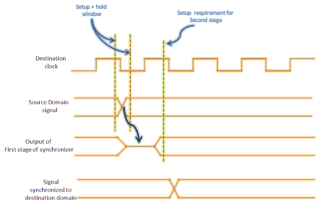
As said earlier, the two flop synchronizer converts a signal from source clock domain to destination clock domain. The input to the first stage is asynchronous to the destination clock. So, the output of first stage (Q1) might go metastable from time to time. However, as long as metastability is resolved before next clock edge, the output of second stage (Q2) should have valid logic levels (as shown in figure 3). Thus, the asynchronous signal is synchronized with a maximum latency of 2 clock cycles.Theoretically, it is still possible for the output of first stage to be unresolved before it is to be sampled by second stage. In that case, output of second stage will also go metastable. If the probability of this event is high, then you need to consider having a three stage synchronizer.


The output of the first stage goes metastable frequently, but there is a great chance of it being resolved before the next clock edge. This is how two-flop synchronizer works.
Waveforms in a two flop synchronizer


A good two flip-flop synchronizer design should have following characteristics:
  • The two flops should be placed as close as possible to allow the metastability at first stage output maximum time to get resolved. Therefore, some ASIC libraries have built in synchronizer stages. These have better MTBF and have very large flops used, hence, consume more power.
  • Two flop synchronizer is the most basic design all other synchronizers are based upon.
  • Source domain signal is expected to remain stable for minimum two destination clock cycles so that first stage is guaranteed to sample it on second clock edge. In some cases, it is not possible even to predict the destination domain frequency. In such cases, handshaking mechanism may be used.
  • The two flop synchronizer must be used to synchronize a single bit data only. Using multiple two flops synchronizers to synchronize multi-bit data may lead to catastrophic results as some bits might pass through in first cycle; others in second cycle. Thus, the destination domain FSM may go in some undesired state.
  • Another practice that is forbidden is to synchronize same bit by two different synchronizers. This may lead to one of these becoming 0, other becoming 1 leading into inconsistent state.
  • The two stages in flop synchronizers are not enough for very high speed clocks as MTBF becomes significantly low (eg. In processors, where clocks run in excess of 1 GHz). In such cases, adding one extra stage will help.
  • MTBF decreases almost linearly with the number of synchronizers in the system. Thus, if your system uses 1000 synchronizers, each of these must be designed with atleast 1000 times more MTBF than the actual reliability target.


Handshaking based synchronizers: As discussed earlier, two flop synchronizer works only when there is one bit of data transfer between the two clock domains and the result of using multiple two-flop synchronizers to synchronize multi-bit data is catastrophic. The solution for this is to implement handshaking based synchronization where the transfer of data is controlled by handshaking protocol wherein source domain places data on the ‘REQ’ signal. When it goes high, receiver knows data is stable on bus and it is safe to sample the data. After sampling, the receiver asserts ‘ACK’ signal. This signal is synchronized to the source domain and informs the sender that data has been sampled successfully and it may send a new data. Handshaking based synchronizers offer a good reliable communication but reduce data transmission bandwidth as it takes many cycles to exchange handshaking signals. Handshaking allows digital circuits to effectively communicate with each other when response time of one or both circuits is unpredictable.

Handshaking protocol based synchronization technique

How handshaking takes place:
1.)    Sender places data, then asserts REQ signal
2.)    Receiver latches data and asserts ACK
3.)    Sender deasserts REQ
4.)    Receiver deasserts ACK to inform the sender that it is ready to accept another data. Sender may start the handshaking protocol again.


Sequence of events in a handshaking protocol based synchronizer


Mux based synchronizers: As mentioned above, two flop synchronizers are hazardous if used to synchronize data which is more than 1-bit in width. In such situations, we may use mux-based synchronization scheme. In this, the source domain sends an enable signal indicating that it the data has been changed. This enable is synchronized to the destination domain using the two flop synchronizer. This synchronized signal acts as an enable signal indicating that the data on data bus from source is stable and destination domain may latch the data. As shown in the figure, two flop synchronizer acts as a sub-unit of mux based synchronization scheme.


A mux based synchronization scheme employs a flop synchronizer internally, to synchronize the control signal to destination domain
A mux-based synchronization scheme


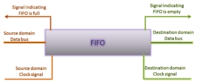
Two clock FIFO synchronizer: FIFO synchronizers are the most common fast synchronizers used in the VLSI industry. There is a ‘cyclic buffer’ (dual port RAM) that is written into by the data coming from the source domain and read by the destination domain. There are two pointers maintained; one corresponding to write, other pointing to read. These pointers are used by these two domains to conclude whether the FIFO is empty or full. For doing this, the two pointers (from different clock domains) must be compared. Thus, write pointer has to be synchronized to receive clock and vice-versa. Thus, it is not data, but pointers that are synchronized. FIFO based synchronization is used when there is need for speed matching or data width matching. In case of speed matching, the faster port of FIFO normally handles burst transfers while slower part handles constant rate transfers. In FIFO based synchronization, average rate into and out of the FIFO are same in spite of different access speeds and types.


A FIFO based synchronizer involves a read-data bus and a write data bus. Also, there are control signals indicating if the FIFO is empty or full
A FIFO based synchronization scheme


Also read: