STA query : How positive edge trigger reg to positive latch path is zero cycle. But positive latch to rising flop is full cycle?

Ever thought why it is expected for setup checks to be single cycle or zero cycle? Common sense prevails that the data launched at any instant is expected to be captured at the next available instant, forming a setup check. We will explain here with the help of an example of latch-to-reg and reg-to-latch path.

Why setup check for postive latch to positive edge-triggered register is full cycle: Figure 1 below shows the clock waveforms for a positive latch to positive edge-triggered flip-flop timing paths. Positive edge-triggered register samples data only on positive edges. In the below figure, those instances are either "Time = 0" or "Time = T". The output of latch can change anytime when it is transparent. The earliest it can change is at "Time = 0+". So, the next instant it can get captured at the register is "Time = T". This makes the default setup check for such paths. That is why setup check for positive latch to positive edge-triggered registers is full cycle.

Figure 1: Single cycle setup check from positive latch to positive edge-triggered flip-flop


Why setup check for positive edge-triggered register to positive level-sensitive latch: Similar to the above case, figure 2 shows the clock wave-forms for positive edge-triggered flip-flop to positive latch timing paths. The flip-flop can launch data at either "Time = 0" or "Time = T". So, data will be available at its output at either "Time = 0+" or "Time = T+". The latch can capture the data at the same instant as it launched as it is transparent at that time. So, setup check is considered to be zero cycle in this case.

Figure 2: Zero cycle setup check from positive edge-triggered flip-flop to positive latch

We need to note that the "from" and "to" edges in these checks denoted in text-books (or shown in timing reports by STA tools by default) are default setup and hold checks. The actual setup and hold check edges are what is represented by the state machine the timing path belongs to. It is possible to ovverride default check edges by command set_multicycle_path. I would recommend going through setup and hold - the state machine essenstials to have a deeper understanding of this concept. In other words, you could have made positive latch to positive edge-triggered flip-flop setup check as single cycle. But you would also have to modify the hold check in that case. Can you guess what it would be?
Design problem: Logic minimization and restructuring for timing critical paths

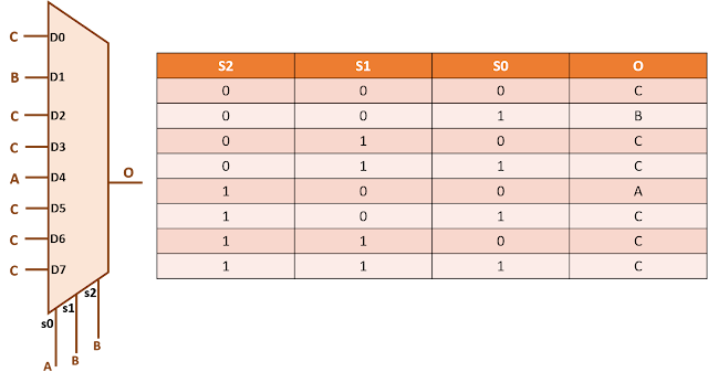
Problem statement: An 8:1 multiplexer selects one out of three inputs based upon different combinations of S2, S1 and S0 as shown in figure below. Minimize the logic with a view that B is the most timing critical input.
Solution:

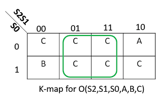
A 4-input MUX has one 4-input AND and one 8-input OR between each input and the output. However, since, there is one signal connected to many of the inputs, there seems to be a scope of logic minimization. Let us use K-map to minimize the logic for problem. The K-map for this problem is as shown below:
Writing the boolean expression, we get:
O = S2'S1'S0' C + S2'S1'S0 B + S1 C + S2S1'S0'A + S2S1'S0 C
O = C (S1 + S1' (S2  ⊕  S0)) + S2'S1'S0 B + S2 S1' S0' A
O = C (S1 + ( S2  ⊕  S0 )) + S2'S1'S0 B + S2 S1' S0' A   [Using A + A'B = A + B]
If we analyze carefully, we see that O is obtained by OR-ing three terms; one for A, one for B and one for C. The resulting structure is shown below:


Since, B is the most timing-critical input; there should be minimum logic between B and output. In other words, it should be closest to output. In the above figure, we see that there is a 4-input AND gate and a 3-input OR gate between and B. We can reduce the logic between B and O by breaking 3-input OR into 2-input OR gates such that B is closest to output. similarly, we can break the 4-input AND gate into 2-input and 3-input AND gates. Thus, we are left with one 2-input AND gate and one 2-input OR gate between B and O as shown in figure below.


We see that there is still a possibility of logic re-structuring between B and O. De-Morgans theorem states that 
A + B = (A' B')'
Going by this, we can convert the OR gate at the output into NAND gate as shown in figure below.

The bubbles at the input of NAND gate can be moved to the outputs of respective drivers. Or, saying, more sophistically, there are two NAND gates between B and O.

Thus, we have achieved our purpose of

  • Minimizing the logic
  • Assuring that there is minimum logic between B and O, since B is the most timing critical input.
We need to keep in mind that there may be more than one solutions to each logic minimization problems. Can you think of a better realization of the circuit in question? What could have been the realization of the circuit in case C was the most timing critical input?