Many a times, two or
more signals at analog-digital interface or at the chip interface have some timing requirement with respect to each other. These requirements are generally in the
form of minimum skew and maximum skew. Data checks come to rescue in such
situations. Theoretically speaking, data-to-data checks are applied between two
arbitrary data signals, none of which is a clock. One of these is called
constrained pin, which is like data pin of the flop. The other is called
related pin, which is like clock pin of the flop. In the figure below, is shown
two data signal at a boundary (possibly analog hard macro) having some minimum
skew requirement between them.
 |
|
Figure 1 : Two signals arriving at a boundary
having skew requirement
|
Data-to-data checks
are zero cycle checks: An important difference between normal setup
check (between a clock signal and a data signal) and data-to-data checks is
that data-to-data checks are zero cycle checks while normal setup check is single cycle check. When we say that
data checks are zero-cycle checks, we mean that these are between two data
signals that have launched at the same clock edge with respect to each other.
As shown in the figure (i) below, traditional setup check is
between a data signal launched at one clock edge and a clock. Since, the data
is launched at one clock edge and is checked with respect to one edge later, it
is a single cycle check. On the other hand, as shown in figure (ii),
data-to-data check is between two signals both of which are launched on the
same clock edge. Hence, we can say
data-to-data checks are zero cycle checks.
 |
|
Figure 2 : (i) Normal setup check between a
data signal and a clock signal, (ii) Data to dat setup check between two data
signals
|
What command in EDA
tools is used to model data-to-data checks: Data checks are
modeled in EDA tools using ‘set_data_check’
command.
Set_data_check –from A –to B –setup <x>
Set_data_check –from A –to B –hold <y>
Here, A is the related pin and B is the constrained pin. The
first command constrains B to toggle at least ‘x’ time before ‘A’. Second command
constrains ‘B’ to toggle at least ‘y’ time after ‘A’.
Data setup time and data hold time: Similar to setup time and hold time, we can define data setup time and data hold time as follows:
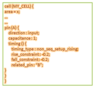
Modeling data-to-data checks through liberty file: We can model data checks through .lib also. There are constructs that can be used to model data-to-data checks. These are non_seq_setup_rising, non_seq_setup_falling, non_seq_hold_rising and non_seq_hold_falling. These commands specify setup and hold data-to-data checks with respect to rising or falling edge of reference signal respectively. E.g. ‘non_seq_setup_falling’ represents data setup check with respect to falling edge of reference signal. ‘rise_constraint’ and ‘fall_constraint’ can be used inside these to model the setup and hold checks for rising and falling edge of constrained signal. Figure 3 below shows an example of modeling data setup check through liberty file.
- Definition of data setup time: Data setup time can be defined as the minimum time before the toggling of reference signal for which constrained signal should become stable. In the example above, <x> is data setup time.
- Definition of data hold time: Data hold time can be defined as the minimum time after the toggling of reference signal for which constrained signal should remain stable. In the example above, <y> is data hold time.
Modeling data-to-data checks through liberty file: We can model data checks through .lib also. There are constructs that can be used to model data-to-data checks. These are non_seq_setup_rising, non_seq_setup_falling, non_seq_hold_rising and non_seq_hold_falling. These commands specify setup and hold data-to-data checks with respect to rising or falling edge of reference signal respectively. E.g. ‘non_seq_setup_falling’ represents data setup check with respect to falling edge of reference signal. ‘rise_constraint’ and ‘fall_constraint’ can be used inside these to model the setup and hold checks for rising and falling edge of constrained signal. Figure 3 below shows an example of modeling data setup check through liberty file.
 |
|
Figure 3 : Modeling data-to-data checks
through .lib using non_seq_setup_rising
|
In which cases
data-to-data checks are applied: Data checks are normally
applied where there is a specific requirement of skew (either minimum of
maximum) or race condition (where the order of arrival of two signals can affect output and the intention is to get one of the probable outputs by constraining one signal to come before the other) between two or more signals. These may be required where:
- At the digital-analog interface within a chip where analog signals at the analog block boundary are required in a specific order
- At the chip boundary, some asynchronous interface signals may have skew requirements
How data checks are useful: As we have seen above, data checks provide a
convenient measure to constrain two or more data signals with respect to each
other. Had these checks not been there, it would have been a manual effort to
check the skew between the two arriving signals and to maintain it. Also, it
would not have been possible to get the optimization done through
implementation tool as these would not have been constrained for it.
References:
- How to constrain the data skew check in the .lib ? - http://tech.tdzire.com/how-to-constrain-the-data-skew-check-in-the-lib/
- Static timing analysis for nanometer designs – a practical approach by J Bhasker and Rakesh Chadha
Also read:
