What DFT is meant
for: Design for Testability (DFT) is basically meant for providing a method
for testing each and every node in the design for structural and other faults.
Higher the number of nodes which can be tested through the targeted number of
patterns, greater is the test coverage of the design. For this to be possible,
every node in the design has to be controllable and observable. But what is
controllability and observability? We can consider these as the two basic
principles of DFT which are to be followed in order to have the maximum test
coverage possible through minimum number of patterns. Let us discuss these.
Controllability:
By controllability from DFT point of view, we intend if both ‘0’ and ‘1’ are able
to propagate to each and every node within the target patterns. A point is said to be controllable if both ‘0’
and ‘1’ can be propagated through scan patterns.
What if a node is
not controllable: To achieve DFT coverage for a node, it is needed to
be controllable. If a node is not controllable, it cannot be tested. For
production mode devices, it is necessary to have certain minimum percentage of
nodes controllable to ensure reliable devices to the customers. So, less number
of controllable nodes mean less DFT coverage, and hence, less reliable devices.
 |
|
Figure 1 : Figure showing a node that
is not controllable within targetted number of patterns
|
Inserting control
points (enhancing controllability): A node can be made controllable by
inserting control points. If the test coverage target is not getting met
through target number of patterns, control points are inserted to increase the
test coverage. A control point is an alternate path supplied to a node to let a
particular value propagate to it. As shown in figure1, NODEA is not
controllable within targeted number of patterns. We need to insert a control
point in order to increase its controllability. As shown in figure2, an
alternate path can be provided to NODEA controlled by enable signal. Adding
control point at NODEA not only improves the controllability of NODEA, but it
also improves the controllability of fanout cone of NODEA.
 |
|
Figure 2 : Inserting control point to
enhance controllability
|
There can be three types of control points:
- ‘0’ control points – Suppose we were earlier able to propagate ‘1’ to NODEA. We only need to let ‘0’ propagate. In that case, we can add a ‘0’ control point
- ‘1’ control points - Suppose we were earlier able to propagate ‘0’ to NODEA. We only need to let ‘1’ propagate. In that case, we can add a ‘0’ control point
- Flop control points – In order to let propagate both ‘0’ and ‘1’ through control points, flops need to be inserted.
In case of ‘0’ and ‘1’ control points, the control input of
mux can be tied to ‘0’ or ‘1’. Hence, area overhead is only a mux. On the other
hand, flop control points come with an overhead of an extra flop.
Observability:
By observability, we mean out ability to measure the state of a logic signal. When
we say that a node is observable, we mean that the value at the node can be
shifted out through scan patterns and can be observed through scan out ports.
What if a node is
not observable: If a node is not observable, it means we cannot see the
value at the node and it is not possible to see the value at that node through
targeted number of patterns. To have scan coverage for the node, it is
necessary to be observable. As in the case of less number of controllable
nodes, if number of observable nodes is less, it means less scan coverage. So,
less number of observable nodes also means less reliable devices. There may be
many cases in which we cannot observe a node. The most common are the nodes
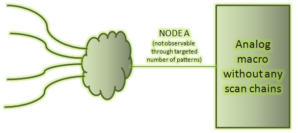
connected to inputs of an analog block not having a scan chain inside. Since,
analog blocks do not have scan chains, the input nodes cannot be observed in
the normal scenario which renders the entire fanin logic unobserved.
 | ||
| Figure 3: Figure showing a non-observable node |
How a node can be
made observable: To improve the observability of nodes in the design,
observe points are inserted. An observe point is a flip-flop inserted in the
design that observes the value at one or more point. It has no functional
purpose. It is inserted in the scan chain and shifts the observed data to scan
out ports through scan shifting. A flip flop inserted as observe point can be
used to observe a large number of hard-to-detect faults which results in a
significant reduction in pattern count.
References:
- Test Point Insertion for Test Coverage Improvement in DFT - http://www.synopsys.com.cn/information/snug/2009/test-point-insertion-for-test-coverage-improvement-in-dft
Also read:

