Power aware RTL design


With the progress in technology, the designs are moving into deeper sub-micron technology nodes. There is an ever-increasing concern about power dissipation within the SoC. But this should not come at the cost of performance. So, along with less power dissipation, there is need for maximum power efficiency, that is maximum proportion of available power should be used for useful purposes rather than just to keep the device awake. Now the question arises: Whether to start planning from power perspective at the RTL Design level or wait for the problems to be fixed in the backend flow of the design cycle. The answer is former. Efforts are made to achieve maximum power efficiency along all the stages of the design. But the backend flow can only implement the changes at physical level. It cannot fix the micro-architecture which has a significant impact on the dynamic power dissipation within the SoC.


Figure showing Impact of design change on performace
Power aware design is achieved at several levels of abstraction. System design starts from system requirements and specification and goes through design at architecture design, RTL design, gate level design and finally, layout design. At all these stages, techniques are adopted to meet the design power and performance requirements. It has been found that any effort that is made to improve the power efficiency along all the design stages has maximum impact, if it is done at the RTL level. But, the impact is measured most immediately if it is done at the layout level. So, it is very difficult to measure the impact of any architectural change at RTL level. Improvements are needed for power estimation methods at the RTL level. But, it does not mean that backend techniques should not be adopted.

Power aware design is often misunderstood as low power design. But, these are not the same. By low power design, we mean minimizing the power consumption with or without any performance constraint. But by power aware design, is meant the minimizing the power dissipation without any impact on power. Power aware design refers to maximizing some other performance constraint without any significant impact on power efficiency. Achieving maximum performance being constrained to a particular power budget is the aim of power aware design. 

As said earlier, there is an ever increasing demand for low power devices. As these devices run on batteries having limited supply, and the requirement for them is to operate the maximum they can on a single battery. There are long phases of device idle time. In between, the device is active for very small periods of time. And during the active time, high performance is the requirement. One such example is digital energy meters where there is requirement to keep record of the total kWh used. The power may be available in patches, or may be continuously available. There may be long periods when there is no power. Since the power is available, we can afford to have chargeable batteries, but the watts consumed by the controller itself should be very less as compared to the total power consumed so as to minimize the overhead. During the idle periods, device may go to sleep mode so as to save power. As long as power is available, it should wake up immediately. In other words, average power is less but variance in power consumption is very high.  Hence, it requires a provision in RTL to sense incoming signal levels and to change the gears accordingly. There are many techniques adopted for power aware RTL designsuch as performance throttling, judicious module selection, incorporation of power information in RTL, voltage and power islands and power aware design of memories.

Read also:

2 bit Binary multiplier


Binary multiplication process: A Binary Multiplier is a digital circuit used in digital electronics to multiply two binary numbers and provide the result as output. The method used to multiply two binary numbers is similar to the method taught to school children for multiplying decimal numbers which is based on calculating partial product, shifting them and adding them together. Similar approach is used to multiply two binary numbers. Long multiplicand is multiplied by 0 or 1 which is much easier than decimal multiplication as product by 0 or 1 is 0 or same number respectively. Figure 1 below shows the block diagram of a 2-bit binary multiplier. The two numbers A1A0 and B1B0 are multiplied together to produce a 4-bit output P3P2P1P0. (The maximum product term can be 3 * 3 = 9, which is 1001, a 4-bit number). 
2-bit Binary multiplier block diagram, 2 bit by 2 bit multiplier, 2 bit multiplier
Figure 1: 2-bit Binary Multiplier Block Diagram
Let us take an example of multiplying two binary numbers as follows. The process is similar to multiplying two decimal numbers, with a difference that the resulting numbers are all binary.

       110 = 6
X     011 = 3
-----------------------------
                                                             1 1 0                 ; 110 X 1
                                                          1 1 0 x                 ; 110 X 1
                                                       0 0 0 x x                 ; 110 X 0
 ------------------------------
 1 0 0 1 0 =18


Now, we have seen that multiplying a number with binary ‘0’produces all zeroes, and with ‘1’ reproduces the number. So, multiplying two binary numbers is a straightforward job. It can be implemented without much difficulty using shifters, AND gates and adders.

2-bit binary multiplier circuit implementation: Let us implement a two bit binary multiplier. Let the two binary numbers be A1A0 and B1B0. The multiplication table will, then, look as:


                                                          A1         A0
                                           X           B1          B0
-------------------------------------------------------------------
                                                      B0A1       B0A0
                                     B1A1         B1A0             x


-------------------------------------------------------------------
                             P3       P2         P1            P0                                  


Thus, we get the partial products as:
P0 = A0*B0
P1 = A0*B1 xor  A1 * B0                  ; carry generated here goes to next stage
P2 = A1*B1   xor  (A0*B1) * (A1*B0)
P3 = A1*B1   and  (A0*B1) * (A1*B0)


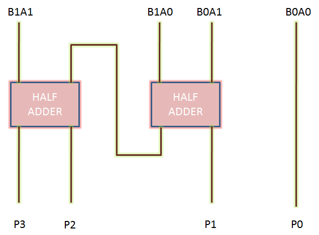
Two bit binary multiplier
Two-bit binary multiplier circuit diagram
Thus, we can see that a 2-bit binary multiplier can be implemented using two half-adders only.

Characteristics of a binary multiplication: As mentioned above, a binary multiplier is used to multiply binary numbers. In general, the characteristics of binary multiplication are as follows:

  • To multiply two binary numbers, AND gates, shifters and adders are required.
  • Product of N*M bit binary numbers in of (N+M) bits.
  •  N*M AND gates are required to generate partial products of two M*N bit binary numbers.
  • Number of adders required =  N+M-2
  • Speed limiting factor here is to sum up  partial products.
Also read: