Carry look ahead adder definition: Carry Look Ahead Adder (CLA Adder) (also known as Carry Look
Ahead Generator) is one of the digital circuits used to implement addition of
binary numbers. It is an
improvement over 'Ripple
carry adder' circuit.
In Ripple Carry adders,
carry propagation time
is the major speed
limiting factor as it works on the
basic mechanism to generate carries as we generally do while adding two numbers
using pen and paper. A ripple carry adder may be supposed to be built of a
series of 1-bit adders (generally known as a full adder in digital
electronics). Thus, the speed of ripple carry adder is a direct function of
number of bits. On the other hand, Carry Look Ahead
adder solves this problem
by calculating carry signals
in advance based upon input
bits and does not wait for the input signal to propagate through
different adder stages. Hence, it implements the adder with reduced delay at
the cost of more area (as large combinational logic is required to calculate
the look ahead carry as compared to propagated carry).
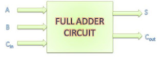
 Shown below is the truth table for a full adder (carry look ahead adder). Ai
and Bi are two input bits and Ci is the carry input
from the previous stage. Si (Sum) and Ci+1 (Carry out for the
next stage) are the outputs for the next stage of the adder. As is evident, carry
signal is generated
if at least two
inputs of full
adder are 1 i.e.
Shown below is the truth table for a full adder (carry look ahead adder). Ai
and Bi are two input bits and Ci is the carry input
from the previous stage. Si (Sum) and Ci+1 (Carry out for the
next stage) are the outputs for the next stage of the adder. As is evident, carry
signal is generated
if at least two
inputs of full
adder are 1 i.e.- When both bits Ai and Bi is 1 (regardless of Cin) OR
- When one of the two inputs (Ai or Bi) is 1 and carry-in (carry of previous stage) is 1
Ai
|
Bi
|
Ci
|
Si
|
Ci+1
|
0
|
0
|
0
|
0
|
0
|
0
|
0
|
1
|
1
|
0
|
0
|
1
|
0
|
1
|
0
|
0
|
1
|
1
|
0
|
1
|
1
|
0
|
0
|
1
|
0
|
1
|
0
|
1
|
0
|
1
|
1
|
1
|
0
|
0
|
1
|
1
|
1
|
1
|
1
|
1
|
The outputs of this full adder, when expressed in the form
of a boolean expression can be written as a function of inputs as follows:
Si
= Ai xor Bi xor Ci
Ci+1 =
Ci(Ai xor Bi) + AiBi
Where Si is the sum bit calculated for nth
adder stage and Ci+1 is the carry out from nth
stage and will act as input for n+1th stage. For an N
stage ripple carry adder, there is overhead of calculating the carry out of kth
stage before carry out of k+1th stage can be calculated. If we go deeper
into analysis, it comes out that ck+1 is a function of c0
and is discussed below. Let the intermediate outputs from a full adder stage be
represented as Pi and Gi given as below:
Pi =
Ai xor Bi
Gi =
Ai.Bi
Si =
Pi xor Ci
Ci+1 =
Ci.Pi + Gi
- Gi is known as carry generate signal since carry (Ci+1)is generated whenever Gi= 1 regardless of Ci
- Pi is known as carry propagate signal since whenever Pi = 1, Ci+1 = Ci (when Pi=1, Gi = 0)
Thus, recursively replacing the values for Ci for each Ck,
we can write the boolean expression
of carry outputs of
various stages in terms of C0 and Pk's as follows:
C1 = C0P0 + G0C2 = C1P1 + G1 = (C0P0+G0)P1 + G1 = C0P0P1 + P1G0 + G1C3 = C2P2 + G2 = (C0P0P1 + P1G0 + G1)P2+G2 = C0P0P1P2 + P2P1G0 + P2G1 + G2C4 = C3P3 + G3 = (C0P0P1P2 + P2P1G0 + P2G1 + G2)P3 + G3 = C0P0P1P2P3 + P3P2P1G0 + P3P2G1 + G2P3 + G3
Thus,
Ci
= F(P,G,C0)
 |
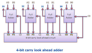
| 4-bit carry look ahead adder block diagram |
A 4 bit Carry
Look Ahead (CLA) adder
can be constructed with the help of following steps (Assuming T as the
delay of a single 2-Input gate):
- Generate All P and G internal signals. These can be generated simultaneously as C0 and all inputs are available.
- Generate all carry output signals (C1, C2, C3, C4). These will be valid after 3T time
- Generate Sum signals S = P xor C. It will be valid after 4T time.
Thus, Sum signals
will be valid after
a delay of 4T. On the other hand, delay expression in
case of ripple carry adder = (2n+2)T. Thus, for n =4, i.e. for 4 bit ripple
carry adder, delay will be 10T.
For higher order addition, boolean
expression of carry output becomes more complex. So, there is tradeoff between area and speed. For larger number of bits, increase in area is more than
speed advantage obtained. Hence, Carry Look Ahead adders are usually implemented as 4-bit
modules that are used to build larger size adders.
Below is a nice video that explains about carry look ahead adders (taken from youtube).
