Showing posts with label CMOS basics. Show all posts

Divide by 2 clock in VHDL

Clock dividers are ubiquitous circuits used in every digital design. A divide-by-N divider produces a clock that is N times lesser frequency as compared to input clock. A flip-flop with its inverted output fed back to its input serves as a divide-by-2 circuit. Figure 1 shows the schematic representation for the same.

A divide by 2 clock circuit produces output clock that is half the frequency of the input clock
Divide by 2 clock circuit
                                          
Following is the code for a divide-by-2 circuit.
-- This module is for a basic divide by 2 in VHDL.
library ieee;
use ieee.std_logic_1164.all;
entity div2 is
                port (
                                reset : in std_logic;
                                clk_in : in std_logic;
                                clk_out : out std_logic
                );
end div2;

-- Architecture definition for divide by 2 circuit
architecture behavior of div2 is
signal clk_state : std_logic;
begin
                process (clk_in,reset)
                begin
                                if reset = '1' then
                                                clk_state <= '0';
                                elsif clk_in'event and clk_in = '1' then
                                                clk_state <= not clk_state;
                                end if;
                end process;
clk_out <= clk_state;

end architecture;

Hope you’ve found this post useful. Let us know what you think in the comments.
Technology scaling factor

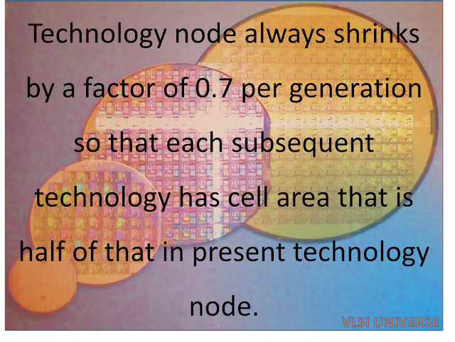
Technology nodex always shrinks by a factor of 0.7 per generation so that each subsequent technology has cell area that is half of that in present technology node.
For instance, you will find technology nodes as 180 um 90 um, 65 um, 45 um, 32 um, 22 um and so on..
*Source - Digital integrated circuits - A design perspective by Jan M Rabay

XOR/XNOR gate using 2:1 MUX

2-input XOR gate using a 2:1 multiplexer: As we know, a 2:1 multiplexer selects between two inputs depending upon the value of its select input. The function of a 2:1 multiplexer can be given as:

OUT = IN0 when SEL = 0 ELSE IN1

Also, a 2-input XOR gate produces a ‘1’ at the output if both the inputs have different value; and ‘0’ if the inputs are same. The truth table of an XOR gate is given as:

A
B
OUT
0
0
0
0
1
1
1
0
1
1
1
0
Truth table of XOR gate

In the truth table of XOR gate, if we fix a value, say B, then

OUT = A WHEN B = 0 ELSE A’


Both the above equations seem equivalent if we connect negative of IN0 to IN1 in a multiplexer. This is how a 2:1 multiplexer will implement an XOR gate. Figure 1 below shows the implement of a 2-input XOR gate using a 2:1 Multiplexer.

An XOR gate can be implemented from a mux simply by connecting the select to one of the inputs, and the inputs to A and Abar respectively.
Implementing a 2-input XOR gate using a 2:1 Multiplexer


I hope you’ve found this post useful. Let me know what you think in the comments. I’d love to hear from you all.


2-input XNOR gate using a 2:1 multiplexer: Similarly, the truth table of XNOR gate can be written as:

A
B
OUT
0
0
1
0
1
0
1
0
0
1
1
1
Truth table of XNOR gate

In the truth table, if we fix, say A, then

OUT = B WHEN A = 1, ELSE B’


Thus, XNOR gate is the complement of XOR gate. It can be implemented if we connect A to IN1 and Abar to IN0.

An XNOR gate can be implemented from a mux simply by connecting the select to one of the inputs, and the inputs to A and Abar respectively.
2-input XNOR gate using 2:1 multiplexer


Read also:

Technology scaling factor

Technology nodex always shrinks by a factor of 0.7 per generation so that each subsequent technology has cell area that is half of that in present technology node.
For instance, you will find technology nodes as 180 um 90 um, 65 um, 45 um, 32 um, 22 um and so on..
*Source - Digital integrated circuits - A design perspective by Jan M Rabay

Can a net have negative propagation delay?


As we discussed in ‘’Is it possible for a logic gate to have negative propagation delay”, a logic cell can have negative propagation delay. However, the only condition we mentioned was that the transition at the output pin should be improved drastically so that 50% level at output is reached before 50% level of input waveform.

In other words, the only condition for negative delay is to have improvement in slew. As we know, a net has only passive parasitic in the form of parasitic resistances and capacitances. Passive elements can only degrade the transition as they cannot provide energy (assuming no crosstalk); rather can only dissipate it. In other words, it is not possible for a net to have negative propagation delay.

However, we can have negative delay for a net, if there is crosstalk, as crosstalk can improve the transition on a net. In other words, in the presence of crosstalk, we can have 50% level at output reached before 50% level at input; hence, negative propagation delay of a net.

Also read:


Depletion MOSFET and negative logic. Why it is not possible?


As we know, depletion MOSFET conducts current even with gate and source at same voltage level. To cut-off the current in depletion MOSFET, a voltage has to be applied at gate so as to exhaust the already existing carriers inside the channel. On the other hand, enhancement type MOSFET is cut-off when gate and source are at same voltage.
Taking the example of NMOS, for a depletion MOS, with source and gate at same level, there is still a channel available, hence, it conducts electric current. To bring it to cut-off, a negative potential is needed to be applied at gate (considering source at ‘X’ potential). Thus, with source at ‘X’ potential and gate at ‘X’ potential, drain attains the potential of source. Since, to cut-off the device, gate has to be given a voltage less than ‘X’, so we can say “when Gate is 1 and source is 1, then drain is 1”.  On the other hand, when source is 1 and gate is 0, drain attains ‘high impedance’. The reverse is true for PMOS.
Similarly, with the same logic, for an enhancement NMOS, “When Gate is 1 and source is 0, drain attains 0 potential”; similarly, “When Gate is 0 and source is 0, drain is 0”. The reverse is true for PMOS.

Source voltage
Gate voltage
Drain voltage for enhancement NMOS
Drain voltage for enhancement PMOS
Drain voltage for depletion NMOS
Drain voltage for depletion PMOS
0
0
Z
Z
0
0
0
1
0
Z
0
Z
1
0
Z
1
Z
1
1
1
Z
Z
1
1

Thus, we can say that it is due to the inherent properties of NMOS and PMOS that that they cannot be used to create negative level logic.

Power aware RTL design


With the progress in technology, the designs are moving into deeper sub-micron technology nodes. There is an ever-increasing concern about power dissipation within the SoC. But this should not come at the cost of performance. So, along with less power dissipation, there is need for maximum power efficiency, that is maximum proportion of available power should be used for useful purposes rather than just to keep the device awake. Now the question arises: Whether to start planning from power perspective at the RTL Design level or wait for the problems to be fixed in the backend flow of the design cycle. The answer is former. Efforts are made to achieve maximum power efficiency along all the stages of the design. But the backend flow can only implement the changes at physical level. It cannot fix the micro-architecture which has a significant impact on the dynamic power dissipation within the SoC.


Figure showing Impact of design change on performace
Power aware design is achieved at several levels of abstraction. System design starts from system requirements and specification and goes through design at architecture design, RTL design, gate level design and finally, layout design. At all these stages, techniques are adopted to meet the design power and performance requirements. It has been found that any effort that is made to improve the power efficiency along all the design stages has maximum impact, if it is done at the RTL level. But, the impact is measured most immediately if it is done at the layout level. So, it is very difficult to measure the impact of any architectural change at RTL level. Improvements are needed for power estimation methods at the RTL level. But, it does not mean that backend techniques should not be adopted.

Power aware design is often misunderstood as low power design. But, these are not the same. By low power design, we mean minimizing the power consumption with or without any performance constraint. But by power aware design, is meant the minimizing the power dissipation without any impact on power. Power aware design refers to maximizing some other performance constraint without any significant impact on power efficiency. Achieving maximum performance being constrained to a particular power budget is the aim of power aware design. 

As said earlier, there is an ever increasing demand for low power devices. As these devices run on batteries having limited supply, and the requirement for them is to operate the maximum they can on a single battery. There are long phases of device idle time. In between, the device is active for very small periods of time. And during the active time, high performance is the requirement. One such example is digital energy meters where there is requirement to keep record of the total kWh used. The power may be available in patches, or may be continuously available. There may be long periods when there is no power. Since the power is available, we can afford to have chargeable batteries, but the watts consumed by the controller itself should be very less as compared to the total power consumed so as to minimize the overhead. During the idle periods, device may go to sleep mode so as to save power. As long as power is available, it should wake up immediately. In other words, average power is less but variance in power consumption is very high.  Hence, it requires a provision in RTL to sense incoming signal levels and to change the gears accordingly. There are many techniques adopted for power aware RTL designsuch as performance throttling, judicious module selection, incorporation of power information in RTL, voltage and power islands and power aware design of memories.

Read also:

­Our world – Digital or analog

Digtal device interfacing with so-called analog worldThere are two kinds of electronic systems that we encounter in our daily life – digital and analog. Digital systems are the ones in which the variables to be dealt with can presume only some specified values whereas in analog systems, these variables can assume any of the infinite values. The superiority of digital devices over analog devices has ever been a topic of discussion. This is the reason why digital devices have taken over analog in almost all the areas that we encounter today. Digital computers, digital watches, digital thermometers etc. have replaced analog computers, analog watches and analog thermometers, and so on. Digital devices have replaced the analog ones due to their superior performance, better ability to handle noise and reliability in spite of being more costly than analog ones. Although most of the devices used today are digital, but in general, the world around us seems to be analog. All the physical quantities around us; i.e. Light, heat, current are analog. The so called digital devices have to interface with this analog real world only. For instance, a digital camera interfaces with analog signal (light) and converts it into information in the form of pixels that collectively form a digital image. Similarly, a music system converts the digital information stored in a music CD into pleasant music which is nothing but analog sound waves. All the digital devices that we know have this characteristic in common. Simply speaking, there are devices known as Analog to Digital converters (ADC) and Digital to Analog converters (DAC) that acts as an interface between the real analog world and the digital devices and converts the data sensed by analog sensor into the digital information understood by the digital system and vice-versa. They all interface with the so called analog world. But is the analog world really analog? Is it true that analog variables can take any number of values? Or is there some limit of granularity for them too. Is this world inherently digital or analog in nature? Is digital more fundamental than analog?
 As we all know, there are many fundamental quantities in this universe viz. Mass, length, time, charge, light etc. We have been encountering these ever since the world has begun. Now the question arises – whether all these quantities are inherently analog or digital? Finding the answer to this question will automatically bring us to the answer of our main question; i.e. whether the basics of this world lie in analog or digital. It is often said that “Heart of digital devices is analog.” (See figure below). This is because, as visible on a macroscopic scale, the current and voltage waveforms produced by a digital circuit/system are not digital in fact. This can be observed from the fact that the transition from one logic state to another cannot be abrupt.  Also, there are small spikes in the voltage levels even if the system is stable in one state. But, seen at microscopic level in terms of transfer of current by transfer of electrons, since, there can only be

transfer of an integral number of electrons, current can only take one of numerous values, and not just any value. Let us take an illustration. The charge on an electron is 1.6E19 (or 0.00000000000000000016) represented as ‘e’. It is the smallest charge ever discovered. It is well known that charge can exist only in the multiples of ‘e’. Thus, electric charge is a digital quantity with the smallest unit ‘e’. When we say that the value of charge at a point is +1C, we actually mean that the charge is caused by transfer of 6250000000000000000 electrons. Since, the smallest unit of charge is 0.00000000000000000016 C, hence, there cannot exist any charge of value 1.00000000000000000015 C, since that will make the number of electrons to be a fraction. Since, the magnitude of 1C is very large as compared to charge on 1e, it appears to us as continuous and not discrete. For us, there is no difference between 1. 00000000000000000015 and 1 as the devices we use don’t measure with that much precision. Hence, we infer these quantities as analog. Similar is the case with other physical quantities.

Many laws have been formed by our great scientists postulating about the quantization of some basic physical quantities. Viz. Planck’s quantum theory states that angular momentum of an electron in the orbit of an atom is quantized. Simply stated, it states that the angular momentum can take only specified values given as multiples of h/2Π. Thus, the smallest angular momentum an electron can have is h/2Π and the angular momentum can increment only in steps of h/2Π. If we take h/2Π as one unit, then we can say that angular momentum of an electron is a digital quantity. Similarly speaking, Light is also known to consist of photons. According to Planck’s quantum theory, the light intensity is also an integral multiple of the intensity of a single photon. Thus, light is also inherently a digital quantity. Also, as stated above, the charge is also quantized.

But there are some physical quantities of which quantization is yet to be established. Mass is one of those quantities. But, it is believed that the quantization of mass will be established soon.

Thus, we have seen that most of the physical quantities known are known to be digital at microscopic level. Since, we encounter these at macroscopic level having billions and billions of basic units, the increments in these seem to be continuous to us as the smallest incremental unit is negligible in comparison to actual measure of the quantity and we perceive them as analog in nature.

Thus, we can come to the conclusion that most of the quantities in this world are digital by their blood. Once the quantization of mass will be established, we can conclude with surety that digital lies in the soul of this world. This digital is similar to our definition of digital systems; just the difference is that it occurs at a very minute scale which we cannot perceive at our own.

Read also: