Metastability tolerant designs

We discussed, in our posts metastability and how a flip-flop goes metastable, the basics of metastability and what causes metastability failures in designs. We also discussed the impacts of metastability failures in our designs. So, we are bound to think of ways of preventing metastability in designs. The only way to do so is not to let the input toggle during setup-hold window. This can be done if we have completely synchronous designs and setup-hold timing is met for all timing paths. But, every design is bound to have asynchronous signals as everything in this world cannot run on a single clock. For example, when you press reset button on a device, this has to be an asynchronous event since the event is generated by your body, which runs on a different clock than the device. :-)

Thus, in reality, we cannot prevent metastability. We can only reduce its existence or make our designs such that the occurence of metastability does not affect the state machine.
  • Avoid metastability to as much extent as possible: As discussed earlier, we can try to make the designs as such synchronous as possible. Thus, by virtue of setup-hold requirements being met, metastability will not be much of an issue. Another possible solution is to decrease the frequency of system. Less number of clock edges will mean less probability of data being captured during setup/hold window. However, do we really want to limit our designs' performance just for the sake of metastability? So, we must make our designs metastability tolerant.
  • Make our designs metastability tolerant to as much extent as possible: The most common way to make designs metastability tolerant is to add synchronizer stages. Doing this, we are allowing certain flip-flops in the design to go metastable, but not allowing their metastability to impact the design by propagating to later stages. However, this also does not guarantee perfect immunity to design failures, but reduces the occurent of design failures due to metastability to almost nil, if carefully designed.

Asynchronous FIFO


ASYNC FIFO is a frequency relationship agnostic bus synchronization technique and by that can be considered practically universal.

It is convenient to choose the write/read pointers of width by one bit bigger than needed by FIFO size. The msb then will play the role of “sign”. The pointers (bus) synchronization is performed with the help of Gray encoding. Gray code encoding is a popular technique to synchronize a bus because only one bit is changed at a time. This ensures we always sample or old or new value on the bus and never – inconsistent one. “g2b” and “b2g” is the logic to convert Gray code to binary and vice versa. It is out of the scope of this article to depict its design.


//write pointer
always @ (src_clk)
      if (!rst_n)
                  wr_ptr <= ‘d0;
      else if (push)
                  wr_ptr <= wr_ptr + 1’b1;
//read pointer
always @ (dst_clk)
      if (!rst_n)
                  rd_ptr <= ‘d0;
      else if (pop)
                  rd_ptr <= rd_ptr + 1’b1;
//full
assign full = (wr_ptr[log(FIFO_SIZE)] ^ rd_ptr_synch[log(FIFO_SIZE)]) &&
(wr_ptr[log(FIFO_SIZE)-1:0] == rd_ptr_synch[log(FIFO_SIZE)-1:0]);
//empty
assign empty = (wr_ptr_synch[log(FIFO_SIZE):0] == rd_ptr[log(FIFO_SIZE):0]);

The important thing to remember is the size of the FIFO has to be exactly power of two. This is because in any other case there will be multiple bit transitions even with Gray code encoding and thus bus synchronization with only one bit changed at a time is violated.


Half-handshake synchronization scheme

Synchronization questions is one of the favorites among VLSI job interviewers. This is because they check not just the general intellectual abilities of the potential candidate but also the very specific professional knowledge which is usually acquired only by experience. When it comes to synchronization there are plenty of schemes. During the emerging interview it often comes to the "ultimate" decision - the synchronizer, which is tolerable to any source-destination conditions (relative frequencies, duration of signals, etc). The expected answer is very well known full-handshake scheme. It is definitely the "ultimate" solution. But its extra-generic nature comes at a cost of very long processing cycle (6 source + 6 destination cycles).

Less known is half hand-shake synchronization scheme which differs from full hand-shake scheme by that it utilizes signals toggling rather than level as an indication to transfer synchronization information from side to side.


At source and destination sides it is toggling (0 to 1 signal change or vice versa) of the synchronized valid signal or ack signal, which becomes an indication the synchronized output may be issued and/or the state changed. Toggled signal may be achieved by comparison (XOR) of the next and current signal value. The current signal value need to be latched at each processing cycle.

Half-handshake scheme provides 2 times better processing cycle than full hand-shake because it consists of only synchronization-acknowledge cycle rather than of synchronization-acknowledge-synchronization de-assertion-acknowledge de-assertion.

How a latch/flip-flop goes metastable

In the post metastability, we discussed that inverter loop can be put into a meta-stable state. Since, latches and flip-flops consist of inverter loops controlled by transmission gates, they also are susceptible to meta-stability. For instance, consider a negative latch as shown in figure 1 and the clock waveform alongside. The instance of interest to us is the instance when switch_1 closes or at the transparency_close edge of the latch. Also, we know from theory two important concepts, "setup time" and "hold time". Let us call the region between setup time and hold time as setup-hold-window. If the data toggles before setup-hold-window, it is guaranteed to get captured and propagated to latch output. If data toggles after setup-hold-window, it is guaranteed not to get propagated to latch output. On the other hand, if it toggles during setup-hold-window, it may or may not propagate to the output. Also, it may happen that when the switch closes, the input level is such that latch goes into metastable state.

Figure 1: How latch goes into metastable state
As is evident from figure 1, input is still transitioning when switch has closed and the output goes metastable.

Similarly, as a flip-flop is also composed of latches configured in master-slave configuration, a flip-flop also goes metastable by same way. In general, we can describe it as:

A flip-flop/latch has a defined timing requirement in terms of when data should be available at its input so that it is correctly captured. These requirements are termed as setup and hold times. If these requirements are not met, there is a possibility of flip-flop going metastable.

In general, following are the scenarios which can cause a flip-flop's output to go metastable.

  • Asynchronous timing paths: Paths crossing clock domains, where the launch and capture clocks do not have definite phase relationship, cannot be assured to be captured outside setup/hold window.
  • If there is a timing path violating setup and/or hold, then the capturing flip-flop will go metastable at a certain PVT, where it is probable to get captured in setup-hold-window
How metastability impacts design:  Let us assume that the output of flip-flop goes to a number of gates (say 100). So, as long as the flip-flop is in metastable range, it will cause short circuit current to flow in all the gates. This link shows the short circuit current to be in the range of 100 uA. So, large amount of short circuit current will flow for a considerable amount of time.


What helps a flip-flop come out of metastability?

As described earlier, theoretically, it is possible for the flip-flop to remain in metastable state for infinite time in the absense of any disturbance. However, there are certain factors, which help it to come out of metastability.


  • Ability of the inverter pair to detect a disturbance and act on it: If the inverter pair is able to detect even a smallest of the disturbances, it will act upon it and eventually come out of metastability. So, having these characteristics for transistors in inverter pair will help:
    • Low VT
    • High drive strength
  • Higher the time available for metastability resolution, more chances of having disturbance; hence, flip-flop will eventuall come out of metastability

In general, the ability of a flip-flop to come out of metastability is measured by a parameter known as MTBF (Mean Time Between Failures). It can be thought of as inverse of failure rate. Higher the MTBF, higher the probability of flip-flop coming out of metastability within a given time. It depends upon:
  • Technology factors
  • Time available to resolve metastability: Higher the time available, higher is MTBF
  • Frequency of the clock received by flip-flop: Higher the frequency of clock, lower is MTBF
  • Frequency of toggling of data received by flip-flop: Higher is frequency of data, lower is MTBF
  • Internal design of flip-flop: Ability of flip-flop to act on smallest of disturbances, as discussed earlier. In general, a flip-flop consuming more power and having high gain will be able to come out of metastability quickly

Metastability

What is metastability: Literally speaking, metastable state refers to a state "which is not so much stable" and a slight disturbance will cause the system to lose state. In the context of VLSI, specifically sequential design, in addition to two stable states "0" and "1", there is also a state in-between at which the output may wander for some time due to inherent feedback design of a latch. This state is known as meta-stable state and the phenomenon is known as metastability. In order to understand this, let us study two back-to-back connected inverters as shown in figure below.

Figure 1: Inverter loop schematic


When the output (N2) of top inverter is 1, M4 & M1 are on. Simlilary, when output is 0, M3 & M2 are on. If the voltage of output inverter is left at anything other than VDD or GND, M4 and M1 try to pull the output towards 1 and the other two pull it towards 0. The final settlement value (either 0 or 1) is dependent upon whose initial pull is stronger. However, if the initial pull combined of M4 & M1 is equal to M3 & M1, the output will not move. The output may or may not remain at this level for some time until equilibrium is maintained. However, if forcefully, we change the output by even a small value, it will settle at 0 or 1 depending upon the direction of forced change. This state is the so-called metastable state. The inverter pair can remain in this state as long as there is no disturbance in the voltage levels. This disturbance can be due to external factors such as external forced voltage or internal factors such as crosstalk. So, if it is left to come out of metastability by itself, the time to come out of metastability is unknown. It depends upon:

  • The value of voltage stimulus: If the level of disturbance is greater than a certain threshold, the output will start to move towards one of the stable levels. Of course, larger the value of initial disturbance, faster will be time to stability
  • Strengths of inverters to pull towards "0" and "1": The less voltage resolution capability the inverter pair has, it will be able to come of metastability in shorter time

How can we generate a pulse for every edge of the incoming pulse

It is a very common requirement to detect either positive edge, negative edge or both edges of a signal. And the circuit that can detect and generate a single cycle pulse is quite simple. In this post, we will discuss how we can detect positive edge, negative edge and both edges of a signal.

  • Detect positive edge of a signal: Positive edge of a signal means that the current state of the signal is "1" and previous state is "0". And a pulse signal means that the output of the circuit is "1" for one cycle. So, we need a circuit which generates "1" as output when present state is "1" and previous state is "0". It generates "0" as output otherwise.
Thus, output = D(n-2)' & D(n-1)
The required implementation is shown in figure 1 below:
Figure 1: Detection of positive edge of signal

  • Detect negative edge of a signal: Negative edge of signal means that the current state of the signal is "0" and previous state is "0". So, we need a circuit which generates "1" as output when present state is "0" and previous state is "1". It generates "0" as output otherwise. 
Thus, Neg_edge_detect = D(n-2) & D(n-1)'
 The required implementation is shown in figure 2 below:
Figure 2: Detection of negative edge of signal


  • Detecting both positive and negative edges of the signal: Simply doing an "OR" operation of Pos_edge_detect and Neg_edge_detect signal will produce an output which is a single cycle pulse for any of the edge of incoming signal. The requirement for consecutive edges of incoming signal is to be at least 2 cycles apart otherwise, the output will not be pulse, but will be a continuous signal.
Any_edge_detect = Pos_edge_detect + Neg_edge_detect
The required implementation is shown in figure 3 below:

Figure 3: Detection of both positive and negative edges of signal

The technique we discussed here delays the output by two cycles. Can you think of any other way to detect the edges of a signal which is more efficient?


Interview questions related to clock jitter and duty cycle variations

Below we list few of our posts related to clock jitter and duty cycle variation. Happy learning.


  • Clock jitter: Disusses the definition and types of clock jitter.
  • Duty cycle of clock: Discusses the definition of duty cycle and how it impacts timing slack of timing paths.
  • Duty cycle variation: Discusses in detail basics of duty cycle variation and its timing implications.

Our purpose is to make this page a single destination for any questions related to clock jitter and duty cycle variation. Please feel free to ask any question related to clock jitter and duty cycle variations.

Interview questions related to reset design and reset timing

Below we list few of our posts related to reset timing and some design concepts related to reset. Happy learning.

Reset basics - Discusses the purpose and design strategies related to reset

Synchronous and asynchronous resets - Discusses the basics of synchronous reset and asynchronous reset. Also discusses few differences between them

Reset synchronizer - Discusses the definition, need and working of reset synchronizers.

Recovery and removal checks - Discusses the timing aspects of asynchronous reset. Provides the definition of recovery check, removal check, recovery time and removal time.

Asynchronous reset assertion timing scenarios - Discusses if there may arise a need to time the assertion of asynchronous resets

Duty cycle care-abouts for clock paths in reset assertion - Discusses how reset assertion can alter the duty cycle of clock, and what needs to be taken care of.

Our purpose is to make this page a single destination for any questions related to reset design and timing. If you have any source of educational information related to reset, please comment or send an email to myblogvlsiuniverse@gmail.com and we will add it here. Also, feel free to ask any question related to reset design and timing.

Does it make sense to check hold violations at synthesis stage

As we know from basics of STA, hold timing equation is generally of the form:

Hold_slack = Data_path_delay - hold_time_of_flop - clock_skew

Which can be re-organized as follows:

Hold_slack = Data_path_delay + launch_clock_delay - capture_clock_delay - hold_time_of_flop

Data_path_delay + launch_clock_delay may be combined to represent arrival of data at the capture flip-flop with respect to clock source. The same is evident from below figure.


The modified equation, then, becomes:
Hold_slack = Data_arrival_at_capture_flop - Clock_arrival_at_capture_flop - hold_time_of_flop
It is clear from above equation that hold checks generally comprise of a race condition between clock and data minus a fixed number (is hold_time_of_flop really a fixed number is a separate question).

Before clock-tree synthesis, we do not have one major aspect of this equation; i.e. we do not know the arrival times of clock at launch and capture flip-flops. Also, we do not know how much is the skew and uncommon clock path contributing to on-chip variations; thus, requiring extra margin for hold slack. Talking about logic synthesis, we do not even have placement data most of the times, so we do not even have correct data path delay estimates with us. So, fixing hold at synthesis will not help as there will anyways be requirement for hold fixes taking into account actual data and clock path delays.

But the most important reason for not fixing hold before clock-tree synthesis is that the task of hold fixing is not much complex for the tools available. It may be as simple as downsizing logic and/or adding buffers in data path where setup slack is available. So, during synthesis and logic placement, tools focus on getting setup targets met and focus on hold after clock tree is built.

Another point to note is that after data nets routing, data path delay may increase because of detouring of data nets as compared to originally estimated. So, it may be wise not to fix hold violations of very small magnitude even after clock-tree synthesis and wait for data nets routing to see how many of those violations are still there.

4:1 mux as universal gate

A universal gate is a gate which can implement any given logic function. NAND and NOR gates are basically known as universal gates, since you can implement any logic function with these. A multiplexer, in a sense, can also be termed as a universal gate, since, you can realize any function by using a mux as a look-up-table structure. In this post, we discuss how we can utilize a 4:1 mux as a universal gate realizing 2-input gates.

Any two-input gate gives a definite value (either 0 or 1) for all the combinations of its inputs and can be represented in the form of truth table as shown in table below.


Here, A,B,C & D can be either "0" or "1" depending upon the functionality of the gate. For instance, for a 2-input AND gate, A = B = C = 0 and D = 1.

Utilizing a 4-input mux for implementing this generic 2-input gate, we can implement as shown below:


For instance, 2-input AND gate will be implemented as following:


This post was written as a response to a query from one of our readers. You can also post your query at post your query.

Duty cycle care-abouts for clock paths in reset assertion

In the post Asynchronous reset assertion timing scenarios, we discussed how we may need to time the assertion of asynchronous reset as well. In this post, we will talk about how important it is to talk about the duty cycle aspect as well. We will use the same example as we did in our previous post to help make a better connection.

In the figure below (discussed in Asynchronous reset assertion timing scenarios), Q0 goes from 0 ->1 and 1 -> 0 in the same cycle, thereby providing a very diminished high pulse, or very diminished low pulse to BIT_1 flip-flop depending upon the delay in reset path of BIT_0 flip-flop. This can result in violation of minimum pulse width requirement of BIT_1. We will discuss this in some detail in this post.

Let us talk only about clock edge number 4. Q0 goes 1 and BIT_1 receives it as positive edge of clock, thereby changing state too. The delay till BIT_1 receiving positive edge of clock is given as

POS_CK_AT_BIT_1 = (Latency of BIT_0) + (CLK->Q of BIT_0) + (BIT_0/Q -> BIT_1/CK)

Now, both Q0 and Q1 go 1, thereby causing the output of NAND gate going "0", which asserts the reset of both BIT_0 and BIT_1. BIT_1 now receives negative edge of clock, whose delay is

NEG_CK_AT_BIT_1 = (Latency of BIT_0) + (CLK->Q of BIT_0) + NAND_DELAY + (R -> Q of BIT_0) +   (BIT_0/Q -> BIT_1/CK)

The width of high pulse that the flip-flop receives is equal to the difference between above two values:
HIGH_PULSE_WIDTH_AT_BIT_1 = NAND_DELAY + (R -> Q of BIT_0)

And low pulse is equal to 
LOW_PULSE_WIDTH_AT_BIT_1 = CLK_PERIOD - HIGH_PULSE_WIDTH_AT_BIT_1

Now, depending upon the combinational delays mentioned as well as CLK_PERIOD, BIT_1 may receive a pulse (either high or low) with width less than what is permissible for its proper functionality. Thus, there will be a pulse width violation.

Looking at the equations for high and low pulse widths, it seems more probable to have high pulse width violating for BIT_1, unless either clock period is very less or buffering is there in reset path of BIT_0. We will need to increase buffering to reset pin of BIT_0 to increase width of high pulse and vice-versa.

The discussion we just had is applicable to any design in particular with reset controlling a signal driving another flip-flop's CK pin. However, one may argue following about this particular circuit:

This particular circuit is resistant to high pulse width violation, but may have low pulse width violations.

Can you argue in favor/against this statement? What is the reason for one making this statement. (Hint: Answer lies in the sequence of events causing CK to BIT_1 to go high and then go low).

Also read:


Asynchronous reset assertion timing scenarios

We have always heard that for asynchronous resets, only de-assertion needs to be timed. This is true for most of the designs as the guidelines followed for implementation of asynchronous resets. However, there may be a  scenario wherein we may need to consider reset assertion as well for our timing checks. In this post, we will try to put some light on it.

In our post "recovery and removal checks", we have elaborated following for asynchronous resets:

* Reset assertion "combinationally" causes the output to go 0; i.e., assertion of reset does not wait for edge of the clock to alter the state of flip-flop

* Reset de-assertion waits for clock edge to propagate the value at "input" to "output". There are checks corresponding to de-assertion of reset with respect to clock known as "recovery" and "removal" checks.

Thus, we see that "recovery" and "removal" checks are defined only for de-assertion of asynchronous reset. So, one must think that there is no timing requirement for reset assertion. This is true in the sense that there is no requirement for reset assertion at the flip-flop that is receiving reset. And overall no timing requirement for a carefully implemented design. But some-times, there may be a corner-case scenario requiring the combinational path throuhg "reset -> output" to be timed. We will discuss some cases to elaborate our statement.

CASE 1: The output of flip-flop goes to another flip-flop, which itself is getting reset at the same time.
Here, since, the output in fanout is itself in reset state, it will not be sampling the output. Hence, there is no need to time the assertion of reset.


CASE 2: The output of flip-flop goes to an asynchronous domain or to a synchronizer which is not, itself, in reset. Here, the asynchronous domain flip-flop is expected to be a synchronizer in most of the cases. So, there does not arise a need for meeting timing.

CASE 3: The output of flip-flop goes to a flip-flop which is working on a synchronous clock and is expecting synchronous data. In this case, we will have to meet timing through the R -> Q of the source flip-flop and getting captured at the destination. We need to keep in mind that reset synchronizer also transfers through R -> Q for reset assertion. So, this case cannot be valid for global asynchronous reset assertion. For instance, let us consider below as a valid scenario.
For below case, we have to meet reset assertion timing from
ASYNC_RESET_SOURCE -> REG_B/R -> REG_B/Q -> REG_C/R -> REG_C/Q -> REG_D/D

Since, reset source is working on asynchronous clock, this is a design violation to get it captured on a flip-flop which is running functionally and expecting synchronous data.

Thus, there may not be any scenario to time asynchronous reset assertion globally. However, the state machines may locally utilize asynchronous reset assertion to get things done. For instance, you must have gone through a common problem known as "conversion of asynchronous counter to decade counter", wherein asynchronous reset pin is utilized to reset the count whenever count reaches 10. We will simplify it as "conversion of 2-bit asynchronous counter to modulo-3 counter" to serve our purpose.

Consider following design of 2-bit asynchronous counter. We have shown two flip-flops to register the output of this counter for illustration purposes and to make the understanding more clear. Flip-flop "BIT_1" gets the output of "BIT_0" as clock. All other flip-flops get CLK as clock. Whenever output of both "BIT_1" and "BIT_0" goes 1, the reset of both flops will cause output to go "00" in the same cycle. This is expected to reach the registers by next clock cycle so that it can be captured properly. The intermediate state "11" is not captured at the next stage as understood by basics of state machines.


We get following timing equations to be met in a single cycle (minus setup time and skews etc.).
BIT_1/CK -> BIT_1/Q -> BIT_1/R -> BIT_1/Q -> REG_1/D
BIT_1/CK -> BIT_1/Q -> BIT_0/R -> BIT_0/Q -> REG_0/D
BIT_0/CK -> BIT_0/Q -> BIT_1/R -> BIT_1/Q -> REG_1/D
BIT_0/CK -> BIT_0/Q -> BIT_0/R -> BIT_0/Q -> REG_0/D

Thus, this is an example of a scenario wherein we need timing for assertion of reset as well. It is captured at the next flip-flops running combinationally through the flip-flops' "Q" pin. Can you deduce the timing paths to be timed for the original case of "asynchronous counter as a decade counter" as well.

Another possible care-about of asynchronous reset assertion may be degradation of duty cycle, if the output is used as a clock such as highlighted path, where Q0 is being consumed as clock for "BIT_1" flip-flop. This can cause the minimum pulse width requirement to be violated for "BIT_1" flip-flop. This perspective of reset assertion is discussed here.

Also read:


Can we use discrete latches and AND/OR gates instead of ICG?

In the post, Integated Clock Gating Cell, we discussed that an ICG has a negative level-sensitive latch preceding an AND gate in order to relax hold timing for clock gating check. And we discussed that it gives benefits for area, power and timing. Let us discuss how area, power and timing are saved. We will discuss only for the case of AND gate, the same will follow for OR gate.

1. Architectural benefits - simplicity in clock handling: By introducing ICGs in place of discrete gates, you dont have to worry about the launch edge of the signal while writing RTL (for details, see here). One can always launch the signal from positive edge-triggered flip-flop for timing and architectural simplicity without worrying about possibility of glitch in clock path due to wrong polarity flip-flop launching enable signal.

2. Benefits in area and power: Having custom module allows for better utilization of resources inside the custom ICG module; hence, it is expected to have lesser power than a latch and an AND gate combined.

3. Benefits in timing: Having the path from latch -> AND inside ICG saves us from having to meet these paths individually, which could take a lot of effort with discrete latch and AND gate. Also, it allows for latch to have almost full time borrow, thereby making almost a full cycle path from a positive edge-triggered flip-flop to ICG.

Also read


Design problem : Convert a multiplexer to priority mux (Logic restructuring for a multiplexer for timing critical paths)

Problem statement: Given an 8:1 multiplexer such that the input connected to 5th input is the most setup timing critical and other inputs are timing critical in the order D0 > D1 > D2 > D3 > D4 > D6 > D7. Restructure the logic accordingly.

Solution: We know that the most setup timing critical signal should have least logic in the data path. So, we need to prioritize 5th input such that it has least logic out of all the inputs. In other words, this is a problem of converting an ordinary multiplexer to a priority multiplexer. Let us first discuss how we can convert a multiplexer to priority mux.

Figure 1 below shows a multiplexer with 8-inputs D0 - D7 and selects S2,S1,S0.
Figure 1: 8:1 multiplexer

The equation for output is given as below:

O = S2.S1.S0.D7 + S2.S1.S0’.D6 + S2.S1’.S0.D5 + S2.S1’.S0’.D4 + S2’.S1.S0.D3 + S2’.S1.S0’.D2 + S2’.S1’.S0.D1 + S2’.S1’.S0’.D0

This multiplexer can be represented in the form of a priority multiplexer as required is as shown in figure 2 below.


We can start from the equation of the priority multiplexer and prove that it is actually equivalent to 8:1 mux.

The equation of the priority multiplexer is given as:

O = (S0.S1'.S2).D5 + (S0.S1'.S2)'.(S0'.S1'.S2').D0 + (S0.S1'.S2)'.(S0'.S1'.S2').(S0.S1'.S2').D1 + (S0.S1'.S2)'.(S0'.S1'.S2').(S0.S1'.S2')'.(S0'.S1.S2').D2           + (S0.S1'.S2)'.(S0'.S1'.S2').(S0.S1'.S2')'.(S0'.S1.S2')'.(S0.S1.S2').D3 + (S0.S1'.S2)'.(S0'.S1'.S2').(S0.S1'.S2')'.(S0'.S1.S2')'.(S0.S1.S2')'.(S0'.S1.S2).D4 + (S0.S1'.S2)'.(S0'.S1'.S2').(S0.S1'.S2')'.(S0'.S1.S2')'.(S0.S1.S2')'.(S0'.S1.S2)'.(S0'.S1.S2).D6 + (S0.S1'.S2)'.(S0'.S1'.S2').(S0.S1'.S2')'.(S0'.S1.S2')'.(S0.S1.S2')'.(S0'.S1.S2)'.(S0'.S1.S2)'.(S0.S1.S2).D7

Simplifying the above equation leads us to the equation of ordinary multiplexer.

Priority multiplexer

Priority multiplexers are common in case one of the inputs is to be prioritized. The reason for this can be either functional or timing. In case of timing being the reason, the most setup timing critical input is connected to the highest priority input. The reason is that the highest priority signal gets the least logic in its path in a priority multiplexer as discussed below. The schematic for a 4-input priority mux is shown in figure 1 below:


In the above diagram, X0 has the highest priority; followed by X1, X2 and X3. A priority multiplexer selects the input if the corresponding select line is "1" and none of the select lines with with higher priority is "1". For example, if S0 is "1", X0 will be selected always. But if S2 is "1", X2 will be selected only if both S1 and S0 are "0".

The logic equation of a priority mux can be written as:

Y = S0.X0 + S0'.S1.X1 + S0'.S1'.S2 X2 + S0'.S1'.S2'.S3.X3 + S0'.S1'.S2'.S3'.S4.X4 + ......

Or, for a 4-input priority mux,

Y = S0.X0 + S0'.S1.X1 + S0'.S1'.S2 X2 + S0'.S1'.S2'.S3.X3

The output of the priority mux is not valid if all the select signals are "0", as we dont know which input to select in that case. That is why, figure 1 shows the D0 of the left multixer as don't care.

How a priority mux differs from a normal mux: In a normal mux, all the inputs have equal priorities, whereas they have different priorities in case of a priority mux.

Design problem: Design a circuit that delays the positive edge of a signal by one cycle

Here, we are given a problem wherein only ( 0 -> 1 ) transition of the signal is delayed by a single clock cycle whereas the other transition changes the output combination-ally. In other words, we are given the task to implement a Mealy state machine as output is both a function of state variables and input. However, this is a pretty simple problem involving single state. The output is a function of:

  • Present input
  • Input value one cycle before

Output should go "0" as soon as input goes "0". But it should go "1" when input one cycle back is "1". But there is a twist. What if current input is "0" and one cycle back, it was "1"? There is no clarity in the problem statement. Let us assume the output remains unchanged in such condition. The state transition table looks as shown below:


We can use K-map to solve for O. The solution is given in the figure below:

The resulting circuit is as shown in figure below.


Can you figure out the circuit that design that delays the negative edge of a signal by one cycle?

Design problem: How do you detect if two 8-bit numbers/signals are equal

Here, the problem involves detecting if each bit of a signal is equal to corresponding bit of the other signal and then generating a resultant. First of all, the circuit which provides equivalence of 1-bit is nothing but an XNOR gate as explained here. So, we require 8 XNOR gates to judge equivalence of individual bits. Even if one of the bits is "0", it means the numbers are not equal, which can be obtained by ANDing the eight bits together.


Alternatively, we can use an XOR gate as well. An XOR gate provides output as "1" if the two inputs are not equal as explained here. Even if one of the 8 individual XOR gates provides output as "1", it will mean that the numbers are not equal, which can be obtained by NORing the eight bits together.


Can you judge which of these can be implemented with less area and power?

Single-bit magnitude comparator

A single-bit magnitude comparator compares between two single-bit values. There can be 4 possible cases for two single bit values A and B as follows:

  • A = B
  • A > B
  • A < B
  • A != B
The truth table showing each of the cases is shown in figure below:


Let us use K-maps for deriving the logic for each of the four outputs as shown in figure below.

Thus, we get

Equation of (A = B) : A (xnor) B
Equation of (A < B) : A' B
 Equation of (A > B) : A B'
Equation of (A != B) : A (xor) B 
 

STA query : How positive edge trigger reg to positive latch path is zero cycle. But positive latch to rising flop is full cycle?

Ever thought why it is expected for setup checks to be single cycle or zero cycle? Common sense prevails that the data launched at any instant is expected to be captured at the next available instant, forming a setup check. We will explain here with the help of an example of latch-to-reg and reg-to-latch path.

Why setup check for postive latch to positive edge-triggered register is full cycle: Figure 1 below shows the clock waveforms for a positive latch to positive edge-triggered flip-flop timing paths. Positive edge-triggered register samples data only on positive edges. In the below figure, those instances are either "Time = 0" or "Time = T". The output of latch can change anytime when it is transparent. The earliest it can change is at "Time = 0+". So, the next instant it can get captured at the register is "Time = T". This makes the default setup check for such paths. That is why setup check for positive latch to positive edge-triggered registers is full cycle.

Figure 1: Single cycle setup check from positive latch to positive edge-triggered flip-flop


Why setup check for positive edge-triggered register to positive level-sensitive latch: Similar to the above case, figure 2 shows the clock wave-forms for positive edge-triggered flip-flop to positive latch timing paths. The flip-flop can launch data at either "Time = 0" or "Time = T". So, data will be available at its output at either "Time = 0+" or "Time = T+". The latch can capture the data at the same instant as it launched as it is transparent at that time. So, setup check is considered to be zero cycle in this case.

Figure 2: Zero cycle setup check from positive edge-triggered flip-flop to positive latch

We need to note that the "from" and "to" edges in these checks denoted in text-books (or shown in timing reports by STA tools by default) are default setup and hold checks. The actual setup and hold check edges are what is represented by the state machine the timing path belongs to. It is possible to ovverride default check edges by command set_multicycle_path. I would recommend going through setup and hold - the state machine essenstials to have a deeper understanding of this concept. In other words, you could have made positive latch to positive edge-triggered flip-flop setup check as single cycle. But you would also have to modify the hold check in that case. Can you guess what it would be?

Design problem: Logic minimization and restructuring for timing critical paths

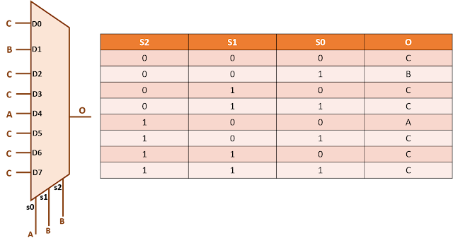
Problem statement: An 8:1 multiplexer selects one out of three inputs based upon different combinations of S2, S1 and S0 as shown in figure below. Minimize the logic with a view that B is the most timing critical input.
Solution:

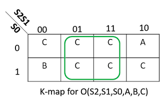
A 4-input MUX has one 4-input AND and one 8-input OR between each input and the output. However, since, there is one signal connected to many of the inputs, there seems to be a scope of logic minimization. Let us use K-map to minimize the logic for problem. The K-map for this problem is as shown below:
Writing the boolean expression, we get:
O = S2'S1'S0' C + S2'S1'S0 B + S1 C + S2S1'S0'A + S2S1'S0 C
O = C (S1 + S1' (S2  ⊕  S0)) + S2'S1'S0 B + S2 S1' S0' A
O = C (S1 + ( S2  ⊕  S0 )) + S2'S1'S0 B + S2 S1' S0' A   [Using A + A'B = A + B]
If we analyze carefully, we see that O is obtained by OR-ing three terms; one for A, one for B and one for C. The resulting structure is shown below:


Since, B is the most timing-critical input; there should be minimum logic between B and output. In other words, it should be closest to output. In the above figure, we see that there is a 4-input AND gate and a 3-input OR gate between and B. We can reduce the logic between B and O by breaking 3-input OR into 2-input OR gates such that B is closest to output. similarly, we can break the 4-input AND gate into 2-input and 3-input AND gates. Thus, we are left with one 2-input AND gate and one 2-input OR gate between B and O as shown in figure below.


We see that there is still a possibility of logic re-structuring between B and O. De-Morgans theorem states that 
A + B = (A' B')'
Going by this, we can convert the OR gate at the output into NAND gate as shown in figure below.

The bubbles at the input of NAND gate can be moved to the outputs of respective drivers. Or, saying, more sophistically, there are two NAND gates between B and O.

Thus, we have achieved our purpose of

  • Minimizing the logic
  • Assuring that there is minimum logic between B and O, since B is the most timing critical input.
We need to keep in mind that there may be more than one solutions to each logic minimization problems. Can you think of a better realization of the circuit in question? What could have been the realization of the circuit in case C was the most timing critical input?


How many 2-input muxes are needed to create an N-input mux

We all know that a 2-input multiplexer selects one out of the available two inputs. Similarly, an N-input multiplexer selects one out of the available N inputs. Now, coming to the answer of the question,

The number of 2-input multiplexers needed to implement an N-input multiplexer is (N-1).

We will arrive at this conclusion by giving an example of an 8-input multiplexer implemented with the help of 2-input multiplexers. Each of the 2-input muxes reduces the number of signals by 1, thereby requiring total of "7" 2-input muxes to implement an 8-input mux.

Let us consider a circuit with 8 inputs and variable outputs. Firstly, if it has 8 outputs, there is no mux in-between.
Figure 1: Circuit with 8 output lines to represent 8 input lines
Now, if we add a 2-input mux between any of the 2 lines, then, we are reducing the number of output lines by 1 as shown in figure 2.
Figure 2: Circuit with 7 output lines and 8 input lines
Simlarly, adding another 2-input mux will leave the number of output lines to be 6. Figure 3 shows two of the all possible configurations of such circuits.
Figure 3: Circuits with 6 output lines and 8 input lines

Similarly, continuing on similar lines, we will need "7" 2-input muxes to converge to a single output. Thus, we can say that "7" 2-input muxes make an 8-input mux.

Similarly, going by this, we will need 13 2-input muxes for a 14:1 mux, 31 for a 32:1 mux, and so on. In other words, (N-1) 2:1 muxes will make up an N-input mux.