Modern VLSI
designs have very complex architectures and multiple clock sources. Multiple
clock domains interact within the chip. Also, there are interfaces that connect
the chip to the outside world. If these different clock domains are not
properly synchronized, metastability events are bound to happen and may result
in chip failure. Synchronizers come to rescue to avoid fatal effects of
metastability arising due to signals crossing clock domain boundaries and are
must where two clock domains interact. Understanding metasbility and correct
design of synchronizers to prevent metastability happen is an art. For systems
with only one clock domain, synchronizers are required only when reading an asynchronous
signal.
Synchronizers, a key to tolerate
metastability: As mentioned earlier, asynchronous signals cause
catastrophic metastability failures when introduced into a clock domain. So,
the first thing that arises in one’s mind is to find ways to avoid
metastability failures. But the fact is that metastability cannot be avoided.
We have to learn to tolerate metastability. This is where synchronizers come to
rescue. A synchronizer is a digital circuit that converts an asynchronous
signal/a signal from a different clock domain into the recipient clock domain
so that it can be captured without introducing any metastability failure.
However, the introduction of synchronizers does not totally guarantee
prevention of metastability. It only reduces the chances of metastability by a
huge factor. Thus, a good synchronizer must be reliable with high MTBF, should
have low latency from source to destination domain and should have low
area/power impact. When a signal is passed from one clock domain to another
clock domain, the circuit that receives the signal needs to synchronize it.
Whatever metastability effects are to be caused due to this, have to be
absorbed in synchronizer circuit only. Thus, the purpose of synchronizer is to
prevent the downstream logic from metastable state of first flip-flop in new
clock domain.
Flip-flop based synchronizer (Two
flip-flop synchronizer): This is the most simple and most common
synchronization scheme and consists of two or more flip-flops in chain working
on the destination clock domain. This approach allows for an entire clock
period for the first flop to resolve metastability. Let us consider the simplest
case of a flip-flop synchronizer with 2 flops as shown in figure. Here, Q2 goes high 1 or 2 cycles
later than the input.
 |
| A two flip-flop synchronizer |
As said earlier,
the two flop synchronizer converts a signal from source clock domain to
destination clock domain. The input to the first stage is asynchronous to the
destination clock. So, the output of first stage (Q1) might go metastable from
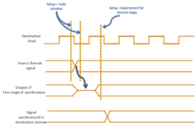
time to time. However, as long as metastability is resolved before next clock
edge, the output of second stage (Q2) should have valid logic levels (as shown
in figure 3). Thus, the asynchronous signal is synchronized with a maximum
latency of 2 clock cycles.Theoretically, it is still possible for the output of
first stage to be unresolved before it is to be sampled by second stage. In
that case, output of second stage will also go metastable. If the probability
of this event is high, then you need to consider having a three stage
synchronizer.
 |
| Waveforms in a two flop synchronizer |
A good two flip-flop
synchronizer design should have following characteristics:
- The two flops
should be placed as close as possible to allow the metastability at first stage
output maximum time to get resolved. Therefore, some ASIC libraries have built
in synchronizer stages. These have better MTBF and have very large flops used,
hence, consume more power.
- Two flop
synchronizer is the most basic design all other synchronizers are based upon.
- Source domain
signal is expected to remain stable for minimum two destination clock cycles so
that first stage is guaranteed to sample it on second clock edge. In some
cases, it is not possible even to predict the destination domain frequency. In
such cases, handshaking mechanism may be used.
- The two flop
synchronizer must be used to synchronize a single bit data only. Using multiple
two flops synchronizers to synchronize multi-bit data may lead to catastrophic
results as some bits might pass through in first cycle; others in second cycle.
Thus, the destination domain FSM may go in some undesired state.
- Another practice
that is forbidden is to synchronize same bit by two different synchronizers.
This may lead to one of these becoming 0, other becoming 1 leading into
inconsistent state.
- The two stages
in flop synchronizers are not enough for very high speed clocks as MTBF becomes
significantly low (eg. In processors, where clocks run in excess of 1 GHz). In
such cases, adding one extra stage will help.
- MTBF decreases
almost linearly with the number of synchronizers in the system. Thus, if your
system uses 1000 synchronizers, each of these must be designed with atleast
1000 times more MTBF than the actual reliability target.
Handshaking based synchronizers: As
discussed earlier, two flop synchronizer works only when there is one bit of
data transfer between the two clock domains and the result of using multiple
two-flop synchronizers to synchronize multi-bit data is catastrophic. The
solution for this is to implement handshaking based synchronization where the
transfer of data is controlled by handshaking protocol wherein source domain
places data on the ‘REQ’ signal. When it goes high, receiver knows data is
stable on bus and it is safe to sample the data. After sampling, the receiver
asserts ‘ACK’ signal. This signal is synchronized to the source domain and
informs the sender that data has been sampled successfully and it may send a
new data. Handshaking based synchronizers offer a good reliable communication
but reduce data transmission bandwidth as it takes many cycles to exchange
handshaking signals. Handshaking allows digital circuits to effectively
communicate with each other when response time of one or both circuits is
unpredictable.
 |
| Handshaking
protocol based synchronization technique |
How
handshaking takes place:
1.) Sender places
data, then asserts REQ signal
2.) Receiver latches
data and asserts ACK
3.) Sender deasserts
REQ
4.) Receiver
deasserts ACK to inform the sender that it is ready to accept another data.
Sender may start the handshaking protocol again.
 |
| Sequence of events in a handshaking protocol based synchronizer |
Mux based synchronizers: As
mentioned above, two flop synchronizers are hazardous if used to synchronize
data which is more than 1-bit in width. In such situations, we may use
mux-based synchronization scheme. In this, the source domain sends an enable
signal indicating that it the data has been changed. This enable is
synchronized to the destination domain using the two flop synchronizer. This
synchronized signal acts as an enable signal indicating that the data on data
bus from source is stable and destination domain may latch the data. As shown
in the figure, two flop synchronizer acts as a sub-unit of mux based synchronization
scheme.
 |
| A mux-based synchronization scheme |
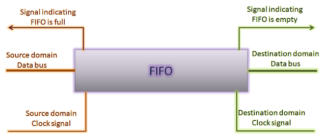
Two clock FIFO synchronizer: FIFO
synchronizers are the most common fast synchronizers used in the VLSI industry.
There is a ‘cyclic buffer’ (dual
port RAM) that is written into by the data coming from the source domain and
read by the destination domain. There are two pointers maintained; one
corresponding to write, other pointing to read. These pointers are used by
these two domains to conclude whether the FIFO is empty or full. For doing
this, the two pointers (from different clock domains) must be compared. Thus,
write pointer has to be synchronized to receive clock and vice-versa. Thus, it
is not data, but pointers that are synchronized. FIFO based synchronization is
used when there is need for speed matching or data width matching. In case of
speed matching, the faster port of FIFO normally handles burst transfers while
slower part handles constant rate transfers. In FIFO based synchronization,
average rate into and out of the FIFO are same in spite of different access
speeds and types.
 |
| A FIFO based synchronization scheme |
Also read:


