Clock skew


Clock skew is one of the most important parameters of a good physical design implementation. Keeping the clock skew to a minimum is considered to be a good measure of clock tree synthesis. 

Definition of clock skew: Clock skew between two flip-flops represents the difference in arrival times of clock signal at the respective clock pins. If there is a timing path being formed between the two flip-flops, then we can attribute a sign to the clock skew. In that case, clock skew is given as:
Clock skew = (Arrival time at capture clock pin) - (Arrival time at launch clock pin)
Thus, based upon the sign of clock skew, we get two types of clock skew labelled as positive skew and negative skew.

Positive clock skew: If the clock arrival time at capture flip-flop is greater than that at launch flip-flop, clock skew is said to be positive. Assuming all buffers take the same delay, figure 1 shows a scenario of positive clock skew.


As shown in figure 1 above for the case of positive clock skew, flip-flop capturing data is getting delayed clock signal. So, the data that is launched gets additional time before it is captured at the next edge. So, setup check gets relaxed by the amount equivalent to clock skew. On the other hand, for hold check, the data has to be kept stable for an extra amount of time equal to the clock skew. So, hold check gets tightened in case clock skew is positive. The same is shown in figure 2 below.


Negative clock skew: Contrary to positive clock skew, if the clock arrival time at capture flip-flop is less than the launch flip-flop, clock skew is said to be negative. Figure 3 shows a scenario of negative clock skew as the launch flip-flop getting a delayed version of clock signal.


Since, the launching flip-flop is getting a delayed version of clock, the data launched gets less than one clock period to travel to the capturing flip-flop. So, negative clock skew makes setup check tighter by the magnitude of clock skew. On the other hand, for hold check, data has to be stable for less time after the arrival of clock edge. In other words, hold check gets relaxed by the same amount. Figure 4 below shows the scenario of negative clock skew.


What makes timing paths both setup critical and hold critical

Those timing paths, which are very hard to meet in timing are called timing critical paths. They can be divided into setup and hold timing critical paths.

Setup timing critical paths: Those paths for which meeting setup timing is difficult, can be termed as setup critical timing paths. For these paths, the setup slack value is very close to zero and for the most part of design cycle, remains below zero.

Hold timing critical paths: As is quite obvious, those paths for which meeting hold timing is difficult, are hold critical paths. These paths may require many buffers to meet hold slack equation.

Sometimes, we may encounter some timing paths which are violating in both setup and hold. There is not enough setup slack to make them hold timing clean and vice-versa. The good practice in timing analysis is to identify all such paths as early as possible in design cycle. Let us discuss the scenarios that make timing paths both setup and hold timing critical.

Inherent frequency limit and delay variations: Let us say, we want our chip to remain functional within following PVTs:
Process : Best-case to Worst-case
Voltage : 1.2 V with 10% voltage variation allowed (1.08 V to 1.32 V)
Temperature : -20 degrees to +150 degress
The delay of a standard cell changes with PVTs and OCVs. Let us only talk about PVT variations. Let us say, cell delay changes by 2 times from worst case scenario (worst process, lowest voltage, worst temperature) to best case scenario (best process, highest voltage, best temperature). Let us say, setup and hold checks also scale by same amount. Remember that the equations for setup and hold need to be satisfied across all the PVTs.  Which essentially means setup needs to be ensured for WCS scenario and hold timing needs to be ensured for BCS scenario. This will provide a limit to maximum frequency that the path can be timed at. If we try to go beyond that frequency, we will not be able to ensure both setup and hold slacks remain positive.

Let us illustrate with the help of an example of a timing path from a positive edge-triggered flip-flop to positive edge-triggered flip-flop with a frequency target of 1.4 GHz (clock time period = 714 ps). Let us say, we have the Best-case and Worst-case scenarios as shown in figure 1 and 2.


Figure 1 shows that the best-case clk->q delay for launch flop is 100 ps, best-case combinational delay is 80 ps and best-case hold time is 200 ps. Applying our hold timing equation for this case,

Hold slack = Tck->q  + Tprop - Thold
Hold slack = 100 + 80 - 200
Hold slack = -20 ps
So, in this case, our hold slack comes out to be negative. So, we need to apply the techniques to improve our hold slack. But we need to ensure that our setup slack is sufficiently positive. Let us look at the worst-case scenario to know about our setup slack. If we assume that everything scales by 2 times, the worst-case numbers for clk->q delay, combinational delay and setup/hold time come out to be 200 ps, 160 ps and 400 ps respectively.


Applying setup timing equation for this scenario,
Setup slack = Tperiod - (Tck->q + Tprop + Tsetup)
Setup slack = 714 - 200 - 160 - 400 = -36 ps 

Thus, for the same timing path, both setup and hold slacks are coming out to be negative. For this path, we cannot meet both setup and hold provided all these conditions. One of the solutions could be to use cells with less delay variability. Or we can limit the operating conditions to a tighter range, for instance, 1.15 to 1.25 V instead. This will improve both setup and hold slack values. If this is not an option, the only option left to satisfy timing is to add delay elements to bring hold slack to zero and reduce the frequency as the inherent variations of cells will not allow the path to operate beyond a certain frequency. Let us check at what maximum frequency our timing path will work.

First, we need to ensure hold timing is met. Thus, 
Hold slack >= 0
This translates to Combinational delay (Cb) > 100 ps, or Cb = 100 ps for a hold slack of 0 ps. In other words, worst case combinational delay is 200 ps (2 times scaling).

For a setup slack of 0 ps, operating clock frequency will be maximum; i.e.,

Tperiod(min) = Tck->q + Tprop + Tsetup
Tperiod(min) = 200+ 200 + 400 = 800 ps 
The minimum time period that it can operate at is 800 ps, or a maximum frequency of 1.25 GHz.

In this post, we have discussed how PVT variations in delay can cause a timing path to be both setup and hold critical. Also, we discussed how it limits the frequency of operation. Although the discussion was limited to only PVT variations, OCV variations will add to the variations. The inherent equations will certainly remain same though. Also, we did not take an important parameter into consideration; i.e. clock skew. Can you think of how clock skew between the two flip-flops contribute to maximum achievable clock frequency? Or is it unrelated to clock skew?


Also read:


Fake currency!!

Problem: A woman goes to buy a pair of shoes. She stops at a shoe store and buys a pair of shoe worth 200 rupees. She hands a thousand rupee note to the shopkeeper. Shopkeeper is short of change, he goes to a nearby tea stall and brings the change. He keeps 200 rupees with himself, handing 800 rupees to the woman. After woman leaves, tea stall owner comes to the shoe store and claims the note to be a fake one. Shoe store owner checks it and agrees. Now the question is, who is in loss and by what amount?

Will post the solution to this puzzle after some time. Till then, let us know your thoughts.

Setup and hold checks

Setup and hold checks ensure that the finite state machine works in the way as designed. In essence, whole of the timing analysis, be it static or dynamic, revolves around setup and hold checks only. In this post, we will be touching upon setup and hold checks.

What is meant by setup check: Setup check ensures that the design transitions to the next state as desired through the state machine design. Mostly, the setup check is at next active clock edge relative to the edge at which data is launched. Let us call this as default setup check. This is, of course, in correspondence to state machine requirement to transfer to next state and the possibility of meeting both setup and hold checks together in view of delay variations accross timing corners. Figure 1 below shows the setup check for a timing path from positive edge-triggered register to negative edge-triggered register. It shows that the data launched by flop1 on positive edge will be captured by flop2 on the forthcoming negative edge and will update the state of flop2. To do so, it has to be stable at the input of flop2 before the negative edge at least setup time before.


Default setup check for positive edge-triggered register to negative edge-triggered register timing path
Figure 1: Default setup check for a timing path from positive edge-triggered to negative edge-triggered flop


What is meant by hold check: Hold check ensures that the design does not move to the next state before its stipulated time; i.e., the design retains its present state only. The hold check should be one active edge prior to the one at which setup is checked unless there are some architectural care-abouts in the state machine design. The hold check corresponding to default setup check in such a scenario is termed as default hold check. Of course, there are some architectural care-abouts for this to happen. Figure 2 below shows the default hold check corresponding to the default setup check of figure 1. It shows that the data launched on positive edge by flop 1 should be captured by next negative edge and not the previous negative edge.


Default hold timing check for a timing path from positive edge-triggered flip-flop to negative edge-triggered flip-flop
Figure 2: Default hold check for a timing path from positive edge-triggered


Default setup and hold check categories: As discussed above, for each kind of timing path, there is a default setup check and a default hold check that will be inferred unless there is an intended non-default check. We can split the setup and hold checks into following categories for our convenience. Each of the following is a link, which you can visit to know about the default setup and hold checks for each category:


Non-default setup and hold checks: These are formed when the state machine behavior is different than the default intended one. Sometimes, a state machine can be designed causing the setup and hold checks to be non-default. For this to happen, of course, you have to first analyze delay variations across timing corners and ensure that the setup timing equation and hold timing equation are satisfied for all timing corner scenarios. The non-default setup and hold checks can be modeled with the help of multi-cycle path timing constraints. You may wish to go through our posts Multicycle paths - the architectural perspective and Multicycle paths handling in STA to understand some of the concepts related to non-default setup and hold checks.

Positive, negative and zero setup time


As we know from the definition of setup time, setup time is a point on time axis which restrains data from changing after it. Data can change only before occurrence of setup timing point. Theoretically, there is no constraint on occurrence of setup time point with respect to clock active edge. It can either be before, after or at the same time as that of clock edge. Depending upon the relative occurrence of setup time point and clock active edge, setup time is said to be positive, zero or negative.

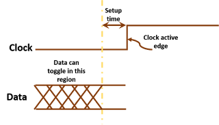
Positive setup time: When setup time point is  before the arrival of clock edge, setup time is said to be positive. Figure 1 below shows positive setup time.
When setup time point is  before the arrival of clock edge, setup time is said to be positive.
Figure 1: Positive setup time


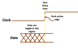
Zero setup time: When setup time point is at the same instant as clock's active edge, setup time is said to be zero. Figure 2 shows a situation wherein setup time is zero.

When setup time point is at the same instant as clock's active edge, setup time is said to be zero.
Figure 2: Zero setup time


Negative setup time: When setup time point occurs after clock edge, setup time is said to be negative. Figure 3 shows timing waveform for negative setup time.
When setup time point occurs after clock edge, setup time is said to be negative.
Figure 3: Negative setup time


What causes different values of setup time: We have discussed above theoretical aspects of positive, zero and negative setup time. Let us go a bit deeper into the details. Figure 4 shows a positive level-sensitive D-latch. As we know from the definition of setup time, setup time depends upon the relative arrival times of data and clock at input transmission gate (We have to ensure data has reached upto NodeD when clock reaches input transmission gate). Depending upon the relative arrival times of data and clock, setup time can be positive, zero or negative.
Figure 4: Positive level-sensitive latch
Let us assume the delay of an inverter is 1 ns. Then, to ensure that the data has reached NodeD when clock edge arrives at input transmission gate, data has to be available at the input transmission gate at least 2 ns before. So, if both data and clock reach the reference point at the same time, the latch has a setup time of 2 ns.

Now, if data takes 1 ns more than clock to reach input transmission gate from the reference point, then, data has to reach reference point at least 3 ns before clock reference point. In this case, setup time will be 3 ns.

Similarly, if data takes 1 ns less than clock to reach input transmission gate, setup time will be 1 ns. And if data takes 2 ns less than clock to reach input transmission gate, setup time will be zero.

Now, if there is further difference between delays of data and clock from respective reference points to input transmission gate, the hold time will become negative. For example, if data takes 3 ns less than clock to reach input transmission gate, setup time will be -1 ns.

This is how setup time depends upon relative delays of data and clock within the sequential element. And it completely makes sense to have negative setup time.

Also read:

Positive, negative and zero hold time


As we know from the definition of hold time, hold time is a point on time axis which restrains data from changing before it. Data can change only after hold time has elapsed. Now, there is no constraint on the occurrence of hold time point with respect to clock edge. It can either be after, before or at the same instant of time as that of clock active edge.

Posotive hold time: When hold time point is after the arrival of clock active edge, hold time is said to be positive hold time. Figure 1 below shows positive hold time.

Positive hold time, hold time, data can toggle after clock edge, data needs to be stable at least for hold time after clock edge
Figure 1: Positive hold time


Zero hold time: When hold time point is at the same time instant as that of clock active edge, we say that hold time of the sequential element is zero. Figure 2 below shows timing waveform for zero hold time.


Data can toggle right after clock edge
Figure 2: Zero hold time


Negative hold time: Similarly, when hold time point comes earlier on time scale as compared to data, we say that hold time of the sequential element is negative. Figure 3 shows timing waveform for negative hold time.

Negative hold time allows data to toggle even before clock ege
Figure 3: Negative hold time


We have discussed above theoretical aspects of positive, zero and negative hold time. Let us go a bit deeper into the details. Figure 4 shows a positive level-sensitive D-latch. As we know (from definition of hold time), hold time depends upon the relative arrival times of clock and data at the input transmission gate (We have to ensure data does not reach NodeC). Depending upon the times of arrival of clock and data, hold time can be positive or negative.

Figure 4: Positive level-sensitive D-latch

Let us say, the delay of an inverter is 1 ns. Then, we can afford the data to reach transmission gate input even 0.9 ns before arrival of clock at transmission gate. This will ensure data reaches NodeC (-0.9 + 1 =) 0.1 n after arrival of clock edge, if allowed. But, since, clock closes transmission gate, data will not reach NodeC. So, in this case, hold time is -1 ns. If the delay from NodeB to NodeC was something else, hold time would also have been different.

Now, if we say that clock arrives at transmission gate 1 ns earlier than data, then, by above logic, hold time of this latch will be -2 ns.

Similarly, if clock arrives at transmission gate 0.5 ns after data, hold time will be -0.5 ns.

And if clock arrive at transmission gate 1 ns after data, hold time will be  zero.

If the arrival time of clock is made more late, hold time will be greater than zero. For example, if arrival time of clock is 2 ns after data, hold time will be +1 ns.


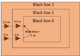
Hold time of the circuit is also dependent upon the reference point. For example, consider a multi-level black box as shown in figure 5. If we look at black box 0, its hold time is -1 ns. At level of black box 1, wherein clock travels 2 ns and data travels 0.5 ns to reach black box 0, hold time is (-1 + 2 - 0.5 = ) 0.5 ns. Similarly, at the level of black box 2, hold time is 1 ns. This is how, hold time depends upon the relative arrival times of clock and data. And it completely makes sense to have a negative hold time.

DFT basics

DFT stands for Design For Testification. DFT engineers try to make the testing of design more cost effective by introducing some structures into the design itself. By doing so, the overall test cost, and hence, cost of production comes down. Below, we list some of our posts covering the basics of DFT. Please provide your feedbacks regarding the topics you want to see as a part of this list. :-) Happy learning.