2-input XOR gate using 2:1 mux

2-input XOR gate using 2x1 mux: Figure 1 shows the truth table for a 2-input XOR gate where A and B are the two inputs and OUT is equal to XOR of A and B. If we observe carefully, OUT equals B when A is '0' and B' when A is '1'. So, a 2:1 mux can be used to implement 2-input XOR gate if we connect SEL to A, D0 to B and D1 to B'.

In a 2-input XNOR gate, output equals '1' when exactly one of the inputs is '1', otherwise output is '0'.
Figure 1: Truth table of 2-input XOR gate
Figure 2 shows the implementation of 2-input XOR gate using 2x1 mux.

A 2-input XNOR gate can be realized using a 2:1 mux provided we connect the select to A-input, D0 to B and D1 to B'. XOR gate using mux, 2-input XNOR gate using mux, XNOR gate using 2:1 mux
Figure 2: Implementation of 2-input XOR gate using 2x1 mux

Similarly, we can connect B to select of mux, and get the XOR gate implemented using similar procedure.

NOT gate using 2:1 mux


NOT gate using 2:1 mux: Figure 13 shows the truth table for a NOT gate. The only inverting path in a multiplexer is from select to output. To implement NOT gate with the help of a mux, we just need to enable this inverting path. This will happen if we connect D0 to '1' and D1 to '0'.

Truth table of NOT gate

Figure 1: Truth table of NOT gate

We can also say that we need to propagate '0' to output when input (select) is 1 and '1' when input is '0'. Figure 14 shows the implementation of NOT gate using 2x1 mux:


A not gate can be implemented by connecting input to the select line of mux. '1' can be connected to D0 and '0' can be connected to D1.
Figure 2: NOT gate implementation using 2:1 mux

Also read:

Zero cycle paths

Zero cycle path: A zero cycle timing path is a representative of race condition between data and clock. A zero cycle path is one in which data is launched and captured on the same edge of the clock. In other words, setup check for a zero cycle path is zero cycle, i.e., it is on the same edge as the one launching data. Hold check, then, will be one cycle before the edge at which data is launched. Figure 1 below shows the setup check and hold check for a zero cycle timing path.


In a zero cycle path, setup check is zero cycle. In other words, it is on the same edge as of launch clock.
Figure 1: Setup check and hold check for zero cycle paths


How to specify zero cycle path: As we know, by default, setup check is single cycle (is checked on the next edge with respect to the one on which data is launched). If the FSM requires a timing path to be zero cycle, it has to be specified using the SDC command "set_multicycle_path".

Default setup check for a timing path is single cycle, whereas hold check is zero cycle.
Figure 2: Default setup and hold checks for single cycle timing path
The default setup and hold check for same edge timing paths is single cycle and zero cycle as shown in figure 2 above. To model it as a zero cycle path (as in figure 1), we need to apply following timing constraint:
set_multicycle_path 0 -setup -from <startpoint> -to <endpoint>
where <startpoint> is the the flip-flop which launches the data and <endpoint> is the flip-flop which captures the data. In other words, as viewed from application perspective, zero cycle path is one of the special cases of a multi-cycle path only. Above multicycle constraint modifies the setup check to be zero cycle. Hold check also, shifts one edge back.

Also read:

XNOR gate using NAND

As we know, the logical equation of a 2-input XNOR gate is given as below:
                      Y = A (xnor) B = (A' B '   +    A B)
Let us take an approach where we consider and A' as different variables for now (optimizations related to this, if any, will consider later). Thus, the logic equation, now, becomes:
                       Y = (CD    +    A B)           -----   (i)
     where
                      C = A'     and      D = B'
De-Morgan's law states that
                                m + n = (m'n')'

Taking this into account,
                     Y = ((CD)'(AB)')' = ((A' B')'  (A B)')'
Thus, Y is equal to ((A' nand B') nand (A nand B)). No further optimizations to the logic seem possible to this logic. Figure 1 below shows the implementation of XOR gate using 2-input NAND gates.
A 2 -input XOR gate implementation using NAND, XOR gate using NAND
Figure 1: 2-input XNOR gate implementation using NAND gates

2x1 mux using NAND gates

As we know, the logical equation of a 2-input mux is given as below:
                      Y = (s' A   +    s B)
Where s is the select of the multiplexer.
De-Morgan's law states that
                                m + n = (m'n')'

Taking this into account, here m = s'A  and  n = sB
                     Y = ((s'A)'(sB)')' = ((s' A)'  (s B)')'
Thus, Y is equal to ((s' nand A) nand (s nand B)). No further optimizations seem possible to this logic. Figure 1 below shows the implementation of 2:1 mux using 2-input NAND gates.
Figure 1: 2:1 Mux using NAND gates

3-input AND gate using 4:1 mux

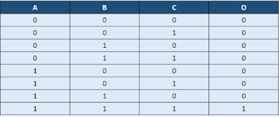
As we know, a AND gate's output goes '1' when all its inputs are '1', otherwise it is '0'. The truth table for a 3-input AND gate is shown below in figure 1, where A, B and C are the three inputs and O is the output.
                                      O = A (and) B (and) C
Truth table for 3-input AND gate


A 4:1 mux has 2 select lines. We can connect A and B to each of the select lines. The output will, then, be a function of the third input C. Now, if we sub-partition the truth table for distinct values of A and B, we observe
When A = 0 and B = 0, O = 0 => Connect D0 pin of mux to '0'
When A = 0 and B = 1, O = 0 => Connect D1 pin of mux to '0'
When A = 1 and B = 0, O = 0 => Connect D2 pin of mux to '0'
When A = 1 and B = 1, O = C => Connect D3 pin of mux to C
The implementation of 3-input AND gate, based upon our discussion so far, is as shown in figure 2 below:


Also read:

3-input XOR gate using 2-input XOR gates


A 3-input XOR gate can be implemented using 2-input XOR gates by cascading 2 2-input XOR gates. Two of the three inputs will feed one of the 2-input XOR gates. The output of the first gate will, then, be XORed with the third input to get the final output.

Let us say, we want to XOR three inputs A,B and C to get the output Z. First, XOR A and B together to obtain intermediate output Y. Then XOR Y and C to obtain Z. The schematic representation to obtain 3-input XOR gate by cascading 2-input XOR gates is shown in figure below:

Implementation of 3-input XOR gate using 2-input XOR gates


Clock gating interview questions

One of the most important and frequently asked topics in interviews is clock gating and clock gating checks. We have a collection of blog-posts related to this topic which can help you master clock gating. You can go through following links to add to your existing knowledge of clock gating:

  • Clock gating checksDiscusses different clock gating structures used and associated timing checks related to these
  • Clock gating checks at a muxDiscusses clock gating checks that should be applied in case one of the inputs of mux has a clock signal connected to it, which is the most common clock gating check in today's designs


Our purpose is to make this page a single destination for any questions related to clock gating. If you have any source of related and additional information, please comment or send an email to myblogvlsiuniverse@gmail.com and we will add it here. Also, feel free to ask any question related to clock gating.