Duty cycle variation of inter-clock timing paths
In the post, duty cycle variation, we understood what duty cycle variation is, and how to apply for intra-clock timing paths. But of similar importance is duty cycle variation as applied to inter-clock timing paths. Let us discuss these cases one-by-one:
Root clock to root-inverted clock: Inverted clock is same as root clock in frequency, with phase inverted. So, duty cycle variation needs to be applied for following cases:

Root clock to odd 50% divided clock: In this scenario, we need to apply extra uncertainty for the following cases:

Root clock to even 50% divided clock: In this case, we need to apply duty cycle uncertainty for the following cases:

So, the rule of thumb is same. Wherever there is a timing path wherein both rising and falling edges of root clock are involved, duty cycle variation will come into play. If you just keep this basic thing into mind, duty cycle variation will never haunt you. :-)
Root clock to root-inverted clock: Inverted clock is same as root clock in frequency, with phase inverted. So, duty cycle variation needs to be applied for following cases:
- Root rise edge -> generated rise edge
- Root fall edge -> generated fall edge
- Generated rise edge -> Root rise edge
- Generated fall edge -> Root fall edge

Following commands will be needed to be applied:
set_clock_uncertainty -rise_from root_clk -rise_to gen_clk <duty_cycle>
set_clock_uncertainty -fall_from root_clk -fall_to gen_clk <duty_cycle>
set_clock_uncertainty -rise_from gen_clk -rise_to root_clk <duty_cycle>
set_clock_uncertainty -fall_from gen_clk -fall_to root_clk <duty_cycle>
Root clock to odd 50% divided clock: In this scenario, we need to apply extra uncertainty for the following cases:
- Root rise edge -> Generated fall edge
- Root fall edge -> Generated rise edge
- Generated rise edge -> Root fall edge
- Generated fall edge -> Root rise edge

Following commands will need to be applied for this case:
set_clock_uncertainty -rise_from root_clk -fall_to gen_clk <duty cycle>
set_clock_uncertainty -fall_from root_clk -rise_to gen_clk <duty cycle>
set_clock_uncertainty -rise_from gen_clk -fall_to root_clk <duty cycle>
set_clock_uncertainty -fall_from gen_clk -rise_to root_clk <duty cycle>
Root clock to even 50% divided clock: In this case, we need to apply duty cycle uncertainty for the following cases:
- Root fall edge -> Generated rise edge
- Root fall edge -> Generated fall edge
- Generated rise edge -> Root fall edge
- Generated fall edge -> Root fall edge
Below figure shows these cases for a 50% divided clock from root clock.

So, the rule of thumb is same. Wherever there is a timing path wherein both rising and falling edges of root clock are involved, duty cycle variation will come into play. If you just keep this basic thing into mind, duty cycle variation will never haunt you. :-)
Also read:
Duty cycle variation
Duty cycle variation: Similar to jitter in clock period, there can be variations in duty cycle of the clock source due to uncertainty in the relative timings of positive and negative edges. Duty cycle variation is always measured with respect to corresponding positive and negative edges. In other words, we can also say that duty cycle variation is the uncertainty in arrival of negative edge, given that positive edge has arrived at certain fixed point of time. Let us take an example. If we are given a clock with a period of 10 ns with ideal 50% duty cycle. Also, we are given that it has the clock has a duty cycle variation of +-5%. So, if we say that we saw positive edge of clock at 100 ns, we can expect to see negative edge of clock at any time between 14.5 ns and 15.5 ns. The timing waveform in figure 2 illustrates this.

Similarly, if we know with certainty, the point of arrival of negative edge, there will be uncertainty in the time of arrival of positive edge of the clock.
Applying duty cycle variation: There may be specific command in STA tools to specify duty cycle variation of a clock. If that is available, you just need to specify duty cycle variation of the master clock source. And all the above discussed cases will be taken care automatically by the tool. If not, it can be applied with the help of SDC command "set_clock_uncertainty". For instance, to apply duty cycle variation for a clock named "clk" of 0.5 ns, we can apply following commands:
set_clock_uncertainty -rise_from clk -fall_to clk 0.5 -setup
set_clock_uncertainty -fall_from clk -rise_to clk 0.5 -setup
set_clock_uncertainty -rise_from clk -fall_to clk 0.5 -hold
set_clock_uncertainty -fall_from clk -rise_to clk 0.5 -hold
Note that there are two commands that need to be applied as there are two categories of half cycle paths, rise-fall and fall-rise.
Timing implication of duty cycle variation: The same way as clock period jitter impacts setup slack of full cycle timing paths; duty cycle variation plays a role in half cycle timing paths. That is why, duty cycle variation is also referred as half cycle jitter. Keeping in mind that there are a lot of cases available with divided and undivided clocks, we will discuss below how to apply duty cycle variation while calculating timing slack. We need to keep in mind that, simlar to full cycle jitter, duty cycle variation is the property of a clock source. With reference to duty cycle variation, there can be following categories of clocks.
Corresponding to these clock categories, there will be multiple cases, some or all of which may be present in your design. And depending upon the scenario, you may need to apply clock uncertainty for that particular case. A simple rule of thumb is that we should apply uncertainty for that scenario wherein the timing path involves both rise and fall edges of master clock. Let us discuss all these one by one:
Intra-clock timing paths:
Duty cycle variation of master clock: For a master clock, there will be a duty cycle variation as specified by the specifications of the clock source. So, if there are half cycle timing paths being formed with respect to this clock, we need to apply clock uncertainty for rise->fall and fall->rise timing paths as suggested by figure below.

- Master clock
- Even divided clocks from master clock with 50% duty cycle
- Odd divided clocks from master clock with 50% duty cycle
- Even divided clocks from inverted master clock with 50% duty cycle
- Odd divided clocks from inverted master clock with 50% duty cycle
- Non-50% divided clocks/arbitrary divided clocks
Corresponding to these clock categories, there will be multiple cases, some or all of which may be present in your design. And depending upon the scenario, you may need to apply clock uncertainty for that particular case. A simple rule of thumb is that we should apply uncertainty for that scenario wherein the timing path involves both rise and fall edges of master clock. Let us discuss all these one by one:
Intra-clock timing paths:
Duty cycle variation of master clock: For a master clock, there will be a duty cycle variation as specified by the specifications of the clock source. So, if there are half cycle timing paths being formed with respect to this clock, we need to apply clock uncertainty for rise->fall and fall->rise timing paths as suggested by figure below.

So, the commands that need to be applied are:
Duty cycle variation of odd divided clock: A divided clock with odd division factor with respect to root clock will have its positive edges aligned with respect to positive edge of root clock; and negative edges aligned to negative edges of root clock. Figure below illustrates this. So, if we assume that the positive edge is fixed (and neglecting clock period jitter), we can say that its negative edges have an uncertainty which is equal to that of root clock.

So, we need to apply following commands for duty cycle variations of odd_div_clock:

Duty cycle variation of arbitrary divided clocks: From the basics we have developed so far, duty cycle variation will be applied to a divided clock if its adjacent edges involve both rising and falling edges of the master clock (as in odd divided clocks) and will not be applied if it involves either only positive or only negative edges of root clock.
Figure below shows an example wherein divide-by-2 clock is generated through clock gating cell. It has a duty cycle of 25%. Here, we need to apply duty cycle variation even as the clock is even divided.

Similarly, if an odd divided clock involves only positive or only negative edges of root clock, duty cycle variation will not apply. Figure below shows an example wherein there is a divide-by-3 clock with 33% duty cycle. Here, we dont need to apply duty cycle variation even though the clock is odd divided.

set_clock_uncertainty <duty_cycle_variation> -rise_from clk -fall_to clk (both for setup and hold)
set_clock_uncertainty <duty_cycle_variation> -fall_from clk -rise_to clk (both for setup and hold)where <duty_cycle_variation> is the duty cycle variation of clock source.
Duty cycle variation of odd divided clock: A divided clock with odd division factor with respect to root clock will have its positive edges aligned with respect to positive edge of root clock; and negative edges aligned to negative edges of root clock. Figure below illustrates this. So, if we assume that the positive edge is fixed (and neglecting clock period jitter), we can say that its negative edges have an uncertainty which is equal to that of root clock.

So, we need to apply following commands for duty cycle variations of odd_div_clock:
set_clock_uncertainty <duty_cycle_variation> -rise_from odd_div_clk -fall_to odd_div_clk
set_clock_uncertainty <duty_cycle_variation> -fall_from odd_div_clk -rise_to odd_div_clkDuty cycle variation of even 50% divided clock: A divided clock with even division factor with respect to root clock will have both its positive and negative edges aligned to positive edge of root clock. Figure below illustrates this. So, for all the intra-clock paths being formed at this clock, duty cycle variation does not apply. This is one of the reasons why emphasis is given to always have even divided clocks in your design.

Duty cycle variation of arbitrary divided clocks: From the basics we have developed so far, duty cycle variation will be applied to a divided clock if its adjacent edges involve both rising and falling edges of the master clock (as in odd divided clocks) and will not be applied if it involves either only positive or only negative edges of root clock.
Figure below shows an example wherein divide-by-2 clock is generated through clock gating cell. It has a duty cycle of 25%. Here, we need to apply duty cycle variation even as the clock is even divided.

Similarly, if an odd divided clock involves only positive or only negative edges of root clock, duty cycle variation will not apply. Figure below shows an example wherein there is a divide-by-3 clock with 33% duty cycle. Here, we dont need to apply duty cycle variation even though the clock is odd divided.

Also read:
Duty cycle of clock
Duty cycle: Duty cycle of a clock is defined as the fraction of a period of clock during which the clock is in active state. Duty cycle of a clock is normally expressed as a percentage. For instance, figure below shows a clock having an active state of '1' stays low for 2 ns during its period of 10 ns. It is, therefore, said to have a duty cycle of 20%.

How duty cycle impacts timing: Duty cycle of clock plays a big role in timing closure of designs. We need to consider following factors related to duty cycle variation while timing:
- Half cycle timing paths: If there are both positive and negative edge-triggered flip-flops in the design, duty cycle of the clock matters a lot. For instance, if we have a clock of 100 MHz with 20% duty cycle; For a timing path from positive edge-triggered flip-flop to negative edge-triggered flip-flop, we get only 2 ns for setup timing for positive-to-negative path and 8 ns for negative-to-positive path as compared to 10 ns for a full cycle path. However, if the same clock had duty cycle of 50%, we would have got 5 ns for the same half cycle timng path.

- Minimum pulse width requirements: At high frequencies, duty cycle matters a lot. For instance, every sequential element has requirement of minimum pulse width that should reach it (read this). If the duty cycle of the clock is not close to 50%, we are limited in providing high frequency even if we are capable of meeting timing at even higher frequencies. Let us take an example. If the minimum pulse width requirement of a flip-flop is 500 ps, then with 50% duty cycle clock, we can use a clock of 1 GHz (1 ns clock period). But if we use a clock of duty cycle of 20%, we cannot use a clock greater than 400 MHz.

With the above things in mind, it makes sense to use a clock with duty cycle as close to 50%. However, in many scenarios, it may not be feasible to do so. So, one needs to decide the priorities; i.e., architecture complexities vs timing complexities. Generating a divided clock of 50% duty cycle is not always possible and there are a few complexities involved in architecture. For instance, clock waveform synchronization between the clocks if there are multiple dividers. Also, for odd division factors like divide_by_3 etc., we need more complex divider circuitry than what may be required for divide_by_2 or divide_by_4 etc.
Which type of jitter matters for timing slack calculation?
In the post Clock jitter, we learnt about the basics of clock jitter. We also learned about different types of clock jitter. Now, the question arises as to what type of clock jitter is useful for calculation of timing slack, both setup and hold slacks. We will gradually try to build understanding for the same.
If we look into the equation of setup slack for a positive edge-triggered flip-flop to another positive edge-triggered flip-flop, we see that setup slack depends upon "clock period". Now, if look closely, we will find that the clock period that we are talking about is actually distance between two clock edges. The larger the distance between the clock edges, greater will be the clock period. Hence, more positive will be setup slack.

Now, period jitter represents the absolute deviation of clock period from its ideal clock period. So, the jitter we should be looking for is maximum value of "peak-to-peak period jitter". Peak-to-peak period jitter can either increase or decrease clock period. But, we need to take the effect of jitter to decrease clock period. This is because we have to take the worst case of clock period to have most pessimistic setup slack value. And the worst clock period will occur when peak-to-peak jitter is maximum.
So, we can say that for setup slack calculation,
What will happen to clock jitter if I divide down the clock?

As we have discussed above, due to clock jitter, for setup calculation, we will assume that peak-to-peak period jitter has caused edge 2 to come closer to edge 1, thereby reducing actual clock period by that margin. Similarly, edge 3 can come closer to edge 2. So, ideally, if we look at DIV_2 clock, the possible jitter here should be 2 times the jitter of SOURCE_CLOCK. Similarly, a DIV_4 clock is expected to have 4 times the jitter and a DIV_8 clock is expected to have 8 times the jitter. And so on..
Now comes the tricky part. As per the definition of long term jitter, nth edge of clock cannot have a jitter more than long term jitter. So, if I say that a PLL has a long term jitter spec of 6 times that of maximum peak-to-peak period jitter, then a DIV_8 clock will have peak-to-peak jitter equal to 6 times the peak-to-peak period jitter of SOURCE_CLOCK. Even a DIV_16 clock will have same maximum jitter.
What will happen to clock jitter for a multicycle path?
Similar to the case of divided down version of clock, a multicycle path also involves other than consecutive edges. So, similar concepts will apply here. So, a multicycle path for setup of 2 will have a jitter of 2 times the peak-to-peak jitter of SOURCE_CLOCK, etc.
If we look into the equation of setup slack for a positive edge-triggered flip-flop to another positive edge-triggered flip-flop, we see that setup slack depends upon "clock period". Now, if look closely, we will find that the clock period that we are talking about is actually distance between two clock edges. The larger the distance between the clock edges, greater will be the clock period. Hence, more positive will be setup slack.

Now, period jitter represents the absolute deviation of clock period from its ideal clock period. So, the jitter we should be looking for is maximum value of "peak-to-peak period jitter". Peak-to-peak period jitter can either increase or decrease clock period. But, we need to take the effect of jitter to decrease clock period. This is because we have to take the worst case of clock period to have most pessimistic setup slack value. And the worst clock period will occur when peak-to-peak jitter is maximum.
So, we can say that for setup slack calculation,
Clock period (actual) = Clock period (ideal) - peak-to-peak jitter (maximum)
What will happen to clock jitter if I divide down the clock?

Now comes the tricky part. As per the definition of long term jitter, nth edge of clock cannot have a jitter more than long term jitter. So, if I say that a PLL has a long term jitter spec of 6 times that of maximum peak-to-peak period jitter, then a DIV_8 clock will have peak-to-peak jitter equal to 6 times the peak-to-peak period jitter of SOURCE_CLOCK. Even a DIV_16 clock will have same maximum jitter.
What will happen to clock jitter for a multicycle path?
Similar to the case of divided down version of clock, a multicycle path also involves other than consecutive edges. So, similar concepts will apply here. So, a multicycle path for setup of 2 will have a jitter of 2 times the peak-to-peak jitter of SOURCE_CLOCK, etc.
Also read:
Clock jitter
Clock jitter: By definition, clock jitter is the deviation of a clock edge from its ideal position in time. Simply speaking, it is the inability of a clock source to produce a clock with clean edges. As the clock edge can arrive within a range, the difference between two successive clock edges will determine the instantaneous period for that cycle. So, clock jitter is of importance while talking about timing analysis. There are many causes of jitter including PLL loop noise, power supply ripples, thermal noise, crosstalk between signals etc. Let us elaborate the concept of clock jitter with the help of an example:
A clock source (say PLL) is supposed to provide a clock of frequency 10 MHz, amounting to a clock period of 100 ns. If it was an ideal clock source, the successive rising edges would come at 0 ns, 100 ns, 200 ns, 300 ns and so on. However, since, the PLL is a non-ideal clock source, it will have some uncertainty in producing edges. It may produce edges at 0 ns, 99.9 ns, 201 ns etc. Or we can say that the clock edge may come at any time between (<ideal_time>+- jitter); i.e. 0, between 99-101 ns, between 199-201 ns etc (1 ns is jitter). However, counting over a number of cycles, average period will come out to be ~100 ns.
Figure 1 below shows the generic diagram for clock jitter:

Please note that the uncertainty in clock edge can be for both positive as well as negative edges (above example showed only for positive edges). So, there are both full cycle and half cycle jitters. By convention, clock jitter implies full cycle clock jitter.
Types of clock jitter: Clock jitter can be measured in many forms depending upon the type of application. Clock jitter can be categorized into cycle-to-cycle, period jitter and long term jitter.

Let us try to understand the difference between all the three kinds of jitter with the help of an illustrative example waveform below:

Reference:
* Understanding SYSCLK jitter
A clock source (say PLL) is supposed to provide a clock of frequency 10 MHz, amounting to a clock period of 100 ns. If it was an ideal clock source, the successive rising edges would come at 0 ns, 100 ns, 200 ns, 300 ns and so on. However, since, the PLL is a non-ideal clock source, it will have some uncertainty in producing edges. It may produce edges at 0 ns, 99.9 ns, 201 ns etc. Or we can say that the clock edge may come at any time between (<ideal_time>+- jitter); i.e. 0, between 99-101 ns, between 199-201 ns etc (1 ns is jitter). However, counting over a number of cycles, average period will come out to be ~100 ns.
Figure 1 below shows the generic diagram for clock jitter:

Please note that the uncertainty in clock edge can be for both positive as well as negative edges (above example showed only for positive edges). So, there are both full cycle and half cycle jitters. By convention, clock jitter implies full cycle clock jitter.
Types of clock jitter: Clock jitter can be measured in many forms depending upon the type of application. Clock jitter can be categorized into cycle-to-cycle, period jitter and long term jitter.
- Cycle to cycle jitter: By definition, cycle-to-cycle jitter signifies the change in clock period accross two consecutive cycles. For instance, it will be difference in periods for 1st and 2nd cycles, difference in periods for 10th and 11th cycles etc. It has nothing to do with frequency variation over time. For instance, in figure below, the clock has drifted in frequency (from period = 10 ns to period = 1 ns), still maintaining a cycle-to-cycle jitter of 0.1 ns. In other words, if t2 and t1 are successive clock periods, then cycle_to_cycle_jitter = (t2 - t1).

- Period jitter: It is defined as the "deviation of any clock period with respect to its mean period". In other words, it is the difference between the ideal clock period and the actual clock period. Period jitter can be specified as either RMS period jitter or peak-to-peak period jitter.
- Peak-to-peak period jitter: It is defined as the jitter value measuring the difference between two consecutive edges of clock. For instance, if the ideal period of the clock was 20 ns, then for clock shown above,
- for first cycle, peak-to-peak period jitter = (20 - 20) = 0 ns
- for second cycle, peak-to-peak period jitter = (20 - 19.9) = 0.1 ns
- for last cyle, peak-to-peak period jitter = (20 - 1) = 19 ns
- RMS period jitter: RMS period jitter is simply the root-mean-square of all the peak-to-peak period jitters available.
- Long term jitter: Long term jitter is the deviation of the clock edge from its ideal position. For instance, for a clock with period 20 ns, ideally, clock edges should arrive at 20 ns, 40 ns and so on. So, if 10th edge comes at 201 ns, we will say that the long term jitter for 10th edge is 1 ns. Similarly, 1000th edge will have a long term jitter of 0.5 ns if it arrives at 20000.5 ns.
Let us try to understand the difference between all the three kinds of jitter with the help of an illustrative example waveform below:

Reference:
* Understanding SYSCLK jitter
Also read:
Post your query
Hi Friends
Please feel free to post your queries as comments. We will try our level best to answer these. You can also write to us at myblogvlsiuniverse@gmail.com.
Please feel free to post your queries as comments. We will try our level best to answer these. You can also write to us at myblogvlsiuniverse@gmail.com.
Can jitter in clock effect setup and hold violations?
First of all, we need to understand what is meant by jitter. In most simplistic language, jitter is the uncertainty of a clock source in production of clock edges. For example, if we say that there is a 100 MHz clock source. Ideally, it should produce a clock edge at 0 ns, 10 ns, 20 ns... So, if we say that there was a clock edge at time t = 30 ns, we should get the next clock edge at t = 40 ns. But this is hardly so; due to the uncertainty of getting a clock edge, we might get the next edge between 39.9 ns to 40.1 ns. So, we say that 0.1 ns is the jitter in the period of the clock. In reality, the definition of jitter is more complex. But, for our scope, this understanding is sufficient.
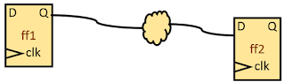
Let us consider a simple timing path from a positive edge-triggered flip-flop to a positive edge-triggered flip-flop.

Now, let us come to our discussion. First, let us discuss the effect of clock jitter on setup slack.
Effect of clock jitter on setup slack for single cycle paths: From our knowledge of STA basics, setup check formed, in this case, will be from edge 1 -> edge 3. Now, if we know that edge 1 arrived at 20 ns, then edge 3 may arrive at any time (20 ns + CLOCK_PERIOD + jitter) and (20 ns + CLOCK_PERIOD - jitter). So, to cover worst case timing scenario, we need to time as per (20 ns + CLOCK_PERIOD - jitter). So, effectively, we will get (CLOCK_PERIOD - jitter) as effective clock period.
 In other words, jitter in clock period makes the setup timing more tight. Or it decreases setup slack for single cycle timing paths.
Effect of clock jitter on hold slack for single cycle paths: Going on the same grounds as setup slack, hold check will be from edge 1 -> edge 1 only. And we know with certainty that edge 1 will leave the source at 20 ns only. So, hold slack should not get bothered by the amount of jitter present at the clock source for single cycle timing paths.
Now, you understand the basics of how jitter affects setup and hold slacks. We can state as below:
If the check being formed involves two different edges of same polarity (for instance, different rising edges), then, jitter in clock period will affect setup slack. Otherwise, it will not.
Now, can you guess the effect of jitter on setup and hold slacks for zero cycle timing paths?
Also, what will be the amount of pessimism needed to be taken into account for setup and hold slacks' calculations if the timing path is a multi-cycle path taking 2 cycles for setup and zero cycle for hold?
Also read:
Recovery and removal checks
Recovery and removal checks are associated with deassertion of asynchronous reset. The assertion of reset causes the output to get reset and deassertion transfers the control of output to clock signal; i.e., deassertion of reset does not change the output as we discussed in post synchronous and asynchronous resets. However, to ensure that the design comes out of reset in deterministic cycle and to avoid metastability, there must be a region around arrival of clock edge within which reset must not be deasserted. This is similar to setup and hold timing checks, the difference being that:
Setup and hold checks are associated with synchronous data signals for a flop and are applied to both rise and fall transitions of data. Recovery and removal checks, on the other hand, are for asynchronous reset transitioning from active state to inactive state only (deassertion of reset).To properly understand what recovery and removal checks are, we need to understand what asynchronous reset assertion and deassertion does.
Asynchronous reset assertion: In a flip-flop, assertion of reset causes the output to go to its reset value (which is normally "0"). The assertion of reset is an asynchronous event and is not impacted by the state of clock. Figure 1 below depicts the assertion of reset. As it can be seen, Output asynchronously goes to "0" as an effect of reset going to its active state "1".

Asynchronous reset deassertion: The deassertion of asynchronous reset causes the output to get out of the impact of reset and behave like a normal flip-flop. When the reset gets deasserted, its output remains to be "0" until the clock edge. When the clock edge arrives, the value at the input of the flop propagates to the output. Figure 2 below depicts the same. However, the position of reset deassertion with respect to clock edge matters here as is the case with setup and hold checks. If the reset toggles in the vicinity of clock edge, the flip-flop may go metastable. This is avoided by defining recovery and removal checks for reset deassertion. For the sake of simplicity, we can say that recovery and removal checks are setup and hold checks for reset deassertion.

Reset recovery check: Recovery check ensures that the deasserted reset signal allows the clock signal to take control of the output at the desired clock edge. For this, reset signal must be stable at least "recovery time" before the active clock edge. Recovery time is the minimum time required between the deassertion of reset signal and arrival of clock edge. This can be modelled similarly as a setup check with the difference of it being a single sided synchronous check only.
Reset removal check: Removal check ensures that the deasserted reset signal does not get captured on the clock edge at which it is launched by reset synchronizer. For this, reset signal must be stable at lease "removal time" after the active clock edge. Removal time is the minimum time required after the arrival of clock edge for which reset must not be deasserted at the flop's reset pin. This can be modelled similarly as a hold check with the difference of it being a single sisded synchronous check only.
Figure below shows reset de-assertion as a complete picture and summarises what we have discussed in this post.

Next read: Reset basics
Also read:
Figure below shows reset de-assertion as a complete picture and summarises what we have discussed in this post.

Next read: Reset basics
Also read:
Synchronous and asynchronous resets
In the post reset basics, we discussed the need of having reset and the strategies used by designers related to reset. One of the decisions that designers need to finalize is to choose synchronous vs asynchronous reset strategy. Each of these reset strategies is capable of achieving the purpose of a reset. A design may also have a mixed approach in which a part of the device is driven by synchronous reset and another part has an asynchronous approach to reset. In this post, we will be discussing the pros and cons of each.
- Synchronous reset: If the reset affects the state of the design only on the active edge of the clock, we term it as a synchronous reset signal. A synchronous reset is fed into the D fanin cone of a flip-flop. Figure 1 below shows a sample design with synchronous reset.

Generally, the reset signal must be closest to the target flip-flop in order to have least number of gates. If the reset of above figure is restructured, one AND gate must be converted to two AND gates to have the reset propagated to the target flip-flop in all situations. But this kind of data path results in increased data path for other critical functional paths. So, synthesis tool needs to take intelligent decision of gate count vs critical signals' timing.
Synchronous reset generation results in smaller flip-flops, but the combinational gate count grows as reset must be applied through combinational logic only.
We can afford to have glitches in reset signal as long as it is meeting setup and hold timing. Therefore, if reset signal is generated by a set of internal logic conditions, synchronous reset is the only goto as there will be glitches formed upon mingling of different conditions.
Reset pulse must be big enough to get captured at the active clock edge target registers. For example, if the register gets launched on a clock of period 5 ns and is targetted for a flip clop receiving a clock of period 20 ns, there is a chance of getting the reset pulse not getting captured. So, there will be a requirement of a pulse stretcher circuit.
There are further complexities when clock gating is implemented to save power. If the clock is gated, you cannot force the design into reset state. Only asynchronous reset can work in that scenario.
- Asynchronous reset: If the reset affects the state of the design asynchronously; i.e., whether or not clock is running, then the design is said to have asynchronous reset.
For designs with asynchronous reset, datapath is independent of reset signal. So, logic levels in datapath are less. This means that we can achieve higher frequency using asynchronous resets.
The design can be reset even when clock is gated. Also, no work arounds are needed during synthesis as in case of synchronous resets.
An asynchronous reset signal needs to be glitch free. Even a small glitch on reset signal can reset the design.
For a flip-flop with asynchronous reset, assertion of reset resets the flip-flop asynchronously. Deassertion of reset leaves the output of flip-flop unchanged. The state of flip-flop will change only on arrival of next clock pulse. There can be two scenarios:
- Clock is gated during deassertion of reset: In this case, we can safely deassert the reset and ungate the clock some time after deassertion.
- Clock is running during deassertion of reset: In this case, we need to take care of the recovery/removal timing of deassertion of reset. The deassertion of reset must be synchronous with respect to clock. Reset synchronizers are needed to synchronize the deassertion of reset signal.
Figure below shows the timing waveform for assertion and deassertion of asynchronous reset. As we can see, the assertion of reset causes the output to go to '0', whereas deassertion waits for the clock edge to arrive and cause the output to change.

Also read:
VLSI - 3
So continuing on the previous post of two current sources in series, this example is important when you analyze lot of circuits.
Lets assume you simulate with ideal current sources
Case 1 : When top current source > lower current source
Since, they are ideal current sources, it happens that they will sink or source that much current ir respective of the voltage across the sources, so it implies that currents may be unequal in single wire and the node potential in between increases.
The reason it increases is that top current source pumps in current but the down source only sinks lesser current, hence forth the rest of the current will charge up the cap at the node and hence forth increases the node potential.
Case 2 : When top current source < lower current source
Since, they are ideal current sources, it happens that they will sink or source that much current ir respective of the voltage across the sources, so it implies that currents may be unequal in single wire and the node potential in between decreases.
The reason it increases is that top current source pumps in lesser current but the down source only sinks higher current, hence forth the rest of the current will be provided by the cap at the node and hence forth decreases the node potential.
Interested studentts should find time in simulating the circuit by replacing the current sources with NMOS and PMOS and understand what will happen.
This is an important step in understanding CMFB.
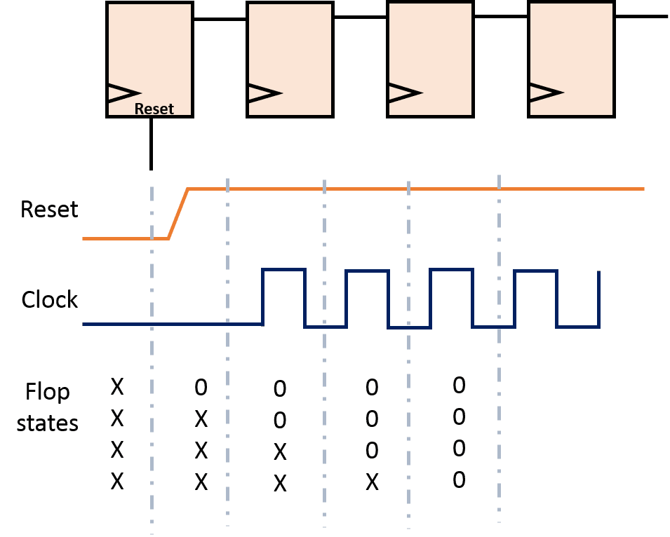
Reset basics
Purpose of reset: We see that almost every electronic device has a reset button. Your video game has a reset button that resets the game and your unsaved progress is lost. Your laptop's reset button reboots it. Have you ever wondered why a system (or specifically a chip) has a reset? Well, the simple purpose of resets is to provide a known initial state to the system to start with. Another reason is, when the system accidentally goes into some unknown state (there may be many reasons for this), the system always knows how to get out of this and go into a known state by asserting a reset signal.
Reset design strategies: Defining a reset is one of the most important decisions that needs to be taken for the good health of design. In general, following things need to be kept in mind during deciding reset strategy:


- What flops to receive reset: One of the easiest and safest approaches is to enable all the flip-flops in the design with a reset. However, there may be a some registers, whose initial state will not have any impact on the design state. In other words, it might not matter if the register's output is '0' or '1' when design goes in reset state. Such registers can be kept non-resettable after an analysis. Let us elaborate with the help of an example. Figure 1 shows a part of an FSM wherein two registers are feeding an AND gate. In figure 1(a), we have decided to initialize both to '0' during reset (with an asynchronous reset, to be explained later). However, given this scenario, if one of the flip-flops is provided with an initial state of '0', the output of the other will be gated. So, we may omit reset on one of the flip-flops. Figure 1(b) shows that omission of reset on one of the flip-flops does not have any impact on state machine design.

We may not always encounter such scenarios. If, instead of AND gate, we had an OR gate, we would not have been able to keep one of the flip-flops uninitialized during reset. Figure 2 shows such an example. In figure 2(b), if we remove reset from second flip-flop, output of OR gate goes 'X'; thus, impacting the state machine.

Another popular scenario wherein we can skip a few registers from having a reset pin is shift registers. If the first stage of a shift register is you give more than one clock pulses when in reset state, subsequent stages will get reset. If you have four stages, you need to give at least three clock pulses while in reset. The same is shown in figure below.
- Synchronous vs asynchronous reset: There are two kinds of reset assertion/deassertion strategies - synchronous vs asynchronous reset. Although each of the two can be used to effective implementation of reset, each of these has its own advantages/disadvantages. Designer may decide upon the desired strategy by considering the pros and cons.
- Synchronous reset means that the reset will affect the state of the design only on the active edge of the clock.
- Asynchronous reset resets the design asynchronously. For this purpose, flip-flops have a special pin that resets the output to '0' or '1' based upon the need.
Clock multiplexer for glitch-free clock switching
In the post clock switching and clock gating checks, we discussed how important it is to have a glitch free clock. Also, in clock gating checks at a multiplexer, we discussed the conditions wherein a normal multiplexer can be used to propagate a clock without any glitches.
In this post, we will discuss about multiplexer circuit for clock switching which can safely switch clocks without the probability of any glitches under most of the scenarios, hence, also called glitch-less multiplexer.
Definition of clock multiplexer: Let us first define a clock multiplexer "A clock multiplexer is a circuit that can switch the system from one clock to another while the chip is running. The two frequencies may be related to each other, or may to totally unrelated". A clock multiplexer switches the clock without any glitches as the glitch in clock will be hazardous for the system. Hence, a clock multiplexer is also known as a glitchless multiplexer.
Clock multiplexer for switching between two synchronous clocks:

Clock multiplexer for switching between two asynchronous clocks:

Reference: A very detailed and good explanation is provided at below link. I recommend to go through this for complete understanding of the process.
http://www.eetimes.com/document.asp?doc_id=1202359
Also read:
http://www.eetimes.com/document.asp?doc_id=1202359
Also read:
STA problem: Finding setup and hold slack taking into accoung clock skew
Problem: Figure 1 below shows a timing path from a positive edge-triggered flip-flop to a positive edge-triggered flip-flop. Considering clock frequency of 200 MHz, find the setup and hold slacks for this timing path.
 |
| Figure 1: Timing path |
As the clock frequency is given as a 200 MHz, time period = 1/frequency = 5 ns.
Let us first calculate the setup slack. The setup timing equation is given as:
Tck->q + Tprop + Tsetup - Tskew < TperiodAnd equation for setup slack is given as:
SS = Tperiod - (Tck->q + Tprop + Tsetup - Tskew)Here,
Tck->q = 2ns, Tprop (max value of delay of combinational logic) = 4 ns+ Tsetup = 1 ns, Tperiod = 5 ns, Tskew = 1 nsPutting these values into equation for setup slack, we get setup slack for this timing path.
SS = 5 - (2 + 4 + 1 - 1) ns
SS = -1 ns
Now, hold slack can be found out from the hold timing equation. The hold timing equation is given as:
Here,Tck->q + Tprop > Thold + Tskew
Tck->q = 2 ns, Tprop (min value of combinational propagation delay) = 4 ns, Thold = 1ns, Tskew = 1 nsAnd the equation for hold slack is given as:
HS = Tck->q + Tprop - (Thold + Tskew)
HS = 2 + 4 - (1 + 1) = 4 nsSo, for this timing path, setup slack value is -1 ns and hold slack value is 4 ns.
STA problem: Finding setup and hold slack considering ideal clock
Problem: Figure 1 below shows a timing path from a positive edge-triggered flip-flop to a positive edge-triggered flip-flop. Considering ideal clocks, and clock frequency of 100 MHz, find the setup and hold slacks for this timing path.
 |
| Figure 1: Timing path |
Ideally, all the flip-flops in design should get clock at the same time. So, ideal clock means that launch as well as capture flip-flops get clock at zero time. In other words, we can assume that clock skew is zero between start and end points.
As the clock frequency is given as a 100 MHz, time period = 1/frequency = 10 ns.
Let us first calculate the setup slack. The setup timing equation is given as:
Tck->q + Tprop + Tsetup - Tskew < TperiodAnd equation for setup slack is given as:
SS = Tperiod - (Tck->q + Tprop + Tsetup - Tskew)Here,
Tck->q = 2ns, Tprop (max value of delay of combinational logic) = 4 ns+ Tsetup = 1 ns, Tperiod = 10 nsPutting these values into equation for setup slack, we get setup slack for this timing path.
SS = 10 - (2 + 4 + 1 - 0) ns
SS = 3 ns
Now, hold slack can be found out from the hold timing equation. The hold timing equation is given as:
Here,Tck->q + Tprop > Thold + Tskew
Tck->q = 2 ns, Tprop (min value of combinational propagation delay) = 4 ns, Thold = 1 nsAnd the equation for hold slack is given as:
HS = Tck->q + Tprop - (Thold + Tskew)
HS = 2 + 4 - (1 + 0) = 5 nsSo, for this timing path, setup slack value is 3 ns and hold slack value is 5 ns.
LVS in VLSI
LVS stands for Layout vs Schematic. It is one of the steps of physical verification; the other one being DRC (Design Rule Check). While DRC only checks for certain layout rules to ensure the design will be manufactured reliably, functional correctness of the design is ensured by LVS.
Layout vs Schematic (LVS) compares the design layout with the design schematic/netlist to tell if the design is functionally equivalent to schematic. For this, the connections are extracted from layout of the design by using a set of rules to convert the layout to connections. These connections are, then compared if they match with the connections of the netlist. If the connections match, the LVS is said to be clean.
VLSI - 2 ( Analog)
For those of you who wanted to make a career in analog, be a devotee of IIT Madras faculty irrespective of which IIT or which college you end up joining for your Mtech.
1. Shanti Pavan - IIT Madras videos
2. Nagendra Krishnapura - IIT Madras videos
3. Razavi - Videos and Text book
4. Anirudhan - IIT Madras videos
I would like to discuss few common blunders, that we end up doing, which henceforth make us loose confidence in analog
In simulation if you put two current sources in series and simulate this, you observe some crazy things happen, kindly do this and learn on this.

Put up a current source with NMOS sinking the current with very low Vgs and observe
Repeat the experiment with PMOS too. Try increasing the sizing for the same Vgs and observe what happens.
This experiments are really the most powerful in analog. The deeper one digs into this, the faster he understands the analog concepts well.
Spend great time dealing with this circuit.
Feel free to discuss if any doubts.......
Will come back with the next post. and discuss the solution and concepts here.
1. Shanti Pavan - IIT Madras videos
2. Nagendra Krishnapura - IIT Madras videos
3. Razavi - Videos and Text book
4. Anirudhan - IIT Madras videos
I would like to discuss few common blunders, that we end up doing, which henceforth make us loose confidence in analog
Mistake 1 : Two current sources in series
In simulation if you put two current sources in series and simulate this, you observe some crazy things happen, kindly do this and learn on this.

Put up a current source with NMOS sinking the current with very low Vgs and observe
Repeat the experiment with PMOS too. Try increasing the sizing for the same Vgs and observe what happens.
This experiments are really the most powerful in analog. The deeper one digs into this, the faster he understands the analog concepts well.
Spend great time dealing with this circuit.
Feel free to discuss if any doubts.......
Will come back with the next post. and discuss the solution and concepts here.
VLSI - 1
Without doubt, VLSI is top branch of ECE which fascinates many graduates and also a hot cake, henceforth making it a very competitive branch to get into even in your Mtech.
Roughly one can divide VLSI into 3 specializations:
Analog VLSI
Digital VLSI
Device Electronics

Analog VLSI --- is something that really fascinates many VLSI students but often, doesn't become a career option for many of those bright students. It is much more than the coding stuff. Analog needs your thinking cap to be on always. It needs understanding of device physics too to a reasonable extent.
Any chip that gets taped out has all blocks of analog, digital. Band gap ckts, Reference current sources, IO components, PLLs, Amplifiers, filters, transmitters, receivers and many blocks are all analog in nature.
Most of the digital stuff are coded and even the interface circuits that is A/D convertors, sensors, and D/A convertors are all analog blocks !!!
The real world is analog in nature and any advancements we talk about DSP, can be appreciated only if u have proper interface circuits to convert the analog signal to digital and do DSP and convert it back to analog again.
Difference between fluorescence and phosphorescence
When electron beam hits phosphorus coated screen, some of the energy of these electrons in dissipated as heat and rest is transferred to electrons of phosphorus which makes them jump to higher energy levels. As we know that higher energy state is unstable and when electron comes to its original state energy is emitted in the form of light(color of light depend upon level from which electrons is returning).
In Ph, some energy levels are less stable than others so electrons in this state returns more rapidly than others.
Hence energy(in the form of light) emitted when these unstable electron return from higher state to its original state while electrons are bombarded on it is called fluorescence.
While the energy emitted when stable electrons return from higher energy levels to its original energy level once electron beam excitation is removed is called phosphorescence.
most of the light emitted in typical Ph is phosphorescence.
Persistence : It is defined as the time from removal of excitation of electron beam to the time when the phosphorescence has decayed to 10% of initial light output. Typically it is between 10-60 microsecond.
How to fix hold violations
In the post setup and hold time violations, we learnt about the setup time violations and hold time violations. In this post, we will learn the approaches to tackle hold time violations. Following strategies can be useful in reducing the magnitude of hold violation and bringing the hold slack towards a positive value:
1. Insert delay elements: This is the simplest we can do, if we are to decrease the magnitude of a hold time violation. The increase in data path delay can be increased if we insert delay elements in the data-path. Thus, the hold violating path's delay can be increased, and hence, slack can be made positive by inserting buffers in hold violating data-path.
2. Reduce the drive strength of data-path logic gates: Replacing a cell with a similar cell of less drive strength will certainly add delay to data-path. However, there is a slight chance of decrease in data-path delay if the cell load is dominated by intrinsic capacitance as we discussed in how delay of a standard cell changes with drive strength
3. Use data-path cells with higher threshold voltages: If you have multiple flavors of threshold voltages in your design, the cells with higher threshold voltage will certainly have higher delays. So, this must be the first option you must be looking for to resolve hold violations.
4. Improve hold time of capturing flip-flop: Using a capturing flip-flop with higher drive strength and/or lower threshold voltage will give a lower hold time requirement. Also, improving the transition at flip-flop's clock pin reduces its hold time requirement.
5. Detoured routing: Detoured routing can be adoped as an alternative to insertion of delay elements as it will add load to the driving cell as well as provide additional net delay thereby increasing the data-path delay.
6. Play with clock skew: A positive skew degrades hold timing and a negative skew aids hold timing. So, if a data-path is violating, we can either decrease the latency of capturing flip-flop or increase the clock latency of launching flip-flop. However, in doing so, we need to keep in mind the setup and hold slacks of other timing paths starting and/or ending at these flip-flops.
7. Increase the clk->q delay of launching flip-flop: A launching flip-flop with more clk->q delay will help ease the hold timing of the data-path. For this, either we can decrease the drive strength of the flip-flop or move it to higher threshold voltage.
Also read:
Also read:
Subscribe to:
Posts (Atom)