Design problem: Logic minimization and restructuring for timing critical paths

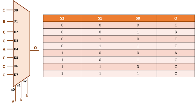
Problem statement: An 8:1 multiplexer selects one out of three inputs based upon different combinations of S2, S1 and S0 as shown in figure below. Minimize the logic with a view that B is the most timing critical input.
Solution:

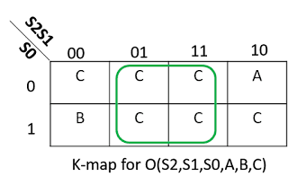
A 4-input MUX has one 4-input AND and one 8-input OR between each input and the output. However, since, there is one signal connected to many of the inputs, there seems to be a scope of logic minimization. Let us use K-map to minimize the logic for problem. The K-map for this problem is as shown below:
Writing the boolean expression, we get:
O = S2'S1'S0' C + S2'S1'S0 B + S1 C + S2S1'S0'A + S2S1'S0 C
O = C (S1 + S1' (S2  ⊕  S0)) + S2'S1'S0 B + S2 S1' S0' A
O = C (S1 + ( S2  ⊕  S0 )) + S2'S1'S0 B + S2 S1' S0' A   [Using A + A'B = A + B]
If we analyze carefully, we see that O is obtained by OR-ing three terms; one for A, one for B and one for C. The resulting structure is shown below:


Since, B is the most timing-critical input; there should be minimum logic between B and output. In other words, it should be closest to output. In the above figure, we see that there is a 4-input AND gate and a 3-input OR gate between and B. We can reduce the logic between B and O by breaking 3-input OR into 2-input OR gates such that B is closest to output. similarly, we can break the 4-input AND gate into 2-input and 3-input AND gates. Thus, we are left with one 2-input AND gate and one 2-input OR gate between B and O as shown in figure below.


We see that there is still a possibility of logic re-structuring between B and O. De-Morgans theorem states that 
A + B = (A' B')'
Going by this, we can convert the OR gate at the output into NAND gate as shown in figure below.

The bubbles at the input of NAND gate can be moved to the outputs of respective drivers. Or, saying, more sophistically, there are two NAND gates between B and O.

Thus, we have achieved our purpose of

  • Minimizing the logic
  • Assuring that there is minimum logic between B and O, since B is the most timing critical input.
We need to keep in mind that there may be more than one solutions to each logic minimization problems. Can you think of a better realization of the circuit in question? What could have been the realization of the circuit in case C was the most timing critical input?
How many 2-input muxes are needed to create an N-input mux

We all know that a 2-input multiplexer selects one out of the available two inputs. Similarly, an N-input multiplexer selects one out of the available N inputs. Now, coming to the answer of the question,

The number of 2-input multiplexers needed to implement an N-input multiplexer is (N-1).

We will arrive at this conclusion by giving an example of an 8-input multiplexer implemented with the help of 2-input multiplexers. Each of the 2-input muxes reduces the number of signals by 1, thereby requiring total of "7" 2-input muxes to implement an 8-input mux.

Let us consider a circuit with 8 inputs and variable outputs. Firstly, if it has 8 outputs, there is no mux in-between.
Figure 1: Circuit with 8 output lines to represent 8 input lines
Now, if we add a 2-input mux between any of the 2 lines, then, we are reducing the number of output lines by 1 as shown in figure 2.
Figure 2: Circuit with 7 output lines and 8 input lines
Simlarly, adding another 2-input mux will leave the number of output lines to be 6. Figure 3 shows two of the all possible configurations of such circuits.
Figure 3: Circuits with 6 output lines and 8 input lines

Similarly, continuing on similar lines, we will need "7" 2-input muxes to converge to a single output. Thus, we can say that "7" 2-input muxes make an 8-input mux.

Similarly, going by this, we will need 13 2-input muxes for a 14:1 mux, 31 for a 32:1 mux, and so on. In other words, (N-1) 2:1 muxes will make up an N-input mux.

4x1 mux using NAND gates

In the post 2x1 mux using NAND gates, we discussed how we can use NAND gates to build a 2x1 multilexer. In this post, we will discuss how we can use NAND gates to build a 4x1 mux:

1. Using structural approach: As we know that a 4x1 mux can be structurally built from 2x1 muxes as shown in figure 1 below. Thus, in the same way, we can arrange the 2-input NAND gates to build 4x1 muxes as shown in figure 1.

Figure 1: 4x1 mux using NAND gates with structural approach


2. Building 4x1 mux directly from NAND gates: The logical equation of a 4x1 multiplexer is given as:
Y = (S1' S0' A + S1' S0 B + S1 S0' C + S1 S0 D)
where S1 and S0 are the selects of the multiplexer and A, B, C and D are the multiplexer inputs.

Now,  using De-morgan's law (m + n = (m'n')')

The above equation turns into,
Y = ((S1' S0' A)'  (S1' S0 B)' (S1 S0' C)' (S1 S0 D)')'
In other words,
Y = NAND (NAND(S1',S0',A),NAND(S1',S0,B),NAND(S1,S0',C),NAND(S1,S0,D)) 
Thus, we require four 3-input NAND gates and a 4-input NAND gate to implement a 4x1 mux. The implementation is shown in figure 2 below.


DESIGN PROBLEM : 4-bit increment by 2 circuit

Problem: Derive the logical expression for a 4-bit increment by 2 circuit and draw the architecture of it.

Solution: The task here is to design a circuit that increments its count by two. Since, it is a 4-bit circuit, the total number of possible states is 16. Each state transitions to the state which has a binary value two greater than it. Now, there are two possible scenarios based upon the initial state that the counter gets into:

1. It can count 0 -> 2 -> 4 -> 6 -> 8 -> 10 -> 12 -> 14 -> 0 (their binary equivalents)

2. It can count 1 -> 3 -> 5 -> 7 -> 9 -> 11 -> 13 -> 15 -> 1 (their binary equivalents)

The state transition table can be represented as shown below:


We can find the expression for outputs using K-maps as below.

Expression for D3(next): Let us first derive the expression for D3(next). The K-map can be represented as below:

The expression for D3(next) as derived from K-map is:
D3(next) = D3.D2' + D3.D1' + D3'.D2.D1
D3(next) = D3.(D2'+D1') + D3'.D2.D1.
D3(next) = D3.(D2.D1)'+D3'.(D2.D1)
D3(next) = D3 (exor) (D2.D1) 

Expression for D2(next): Given below is the K-map derived from state transition table for D2(next).


The expression for D2(next) as derived from K-map is:
D2(next) = D2'.D1 + D2.D1' = D2 (exor) D1

Expression for D1(next):  Given below is the K-map derived from state transition table for D1(next).

The expression for D1(next) is derived from K-map as:
D1(next) = D1'

Expression for D0(next): Given below is the K-map for D0(next).

The expression for D0(next) is:
D0(next) = D0

Combining all the expressions, the circuit is as given below:


Can you come up with a better solution for this problem? Let us know your views in comments.

This question was asked by one Himadri Roy Pramanik on our post your query page. You can also post your queries there. We will try to answer using our limited knowledge.

Clock gating checks in case of mux select transition when both clocks are running

PROBLEM: In the following figure, it is desired to toggle the select of the mux from CLOCK_DIV to CLOCK and both the clocks are running. What are the architectural and STA considerations for the same?

SOLUTION:
This is a very good example to understand how clock gating checks work, although you may/may not find any practical application for the same. We have to toggle the select of the multiplexer such that there is no glitch at the output. Let us consider architectural considerations first:

Architectural considerations:

Launching flip-flop of 'select' signal: In the post clock gating checks at a multiplexer, we discussed that if there is a mux getting clock at its inputs and select as data, then, there are two possible scenarios:

  • If the other clock is at state "0", then AND type check is formed and select has to launch from negative edge-triggered flip-flop
  • If the other clock is at state "1", then OR type check is formed and select has to launch from positive edge-triggered flip-flop
Now, since both the clocks are running simultaneously, both with act as "other clock" for each other. Let us choose to keep both the clocks at state "0" when select toggles. The same discussion holds true for the other scenario as well, just that appropriate values will hold. Thus,

(i) Both clocks required to be at state '0' when clock toggles
(ii) There is AND-type clock gating check formed between 'select' and both clocks 
(iii) 'select' launches from negative edge-triggered flip-flop.


Valid negative edges when 'select' can toggle: Now, as mentioned above both the clocks should be zero when select toggles. Figure below shows the valid and invalid edges where 'select' can toggle. As it turns out, select can toggle only on edges labelled "VALID" as both "CLOCK" and "DIV_CLOCK" will be zero then.

 So, to ensure that "SEL" toggles only when DIV_CLOCK is "0", we can add logic to the input of the flip-flop launching "SEL" such that it allows to propagate "SEL" only when DIV_CLOCK is "0".


In the above diagram, flip-flop launching "SEL" will hold its value when DIV_CLOCK = 0. We have to keep in mind that this implementation is just a representation of what needs to be done. the actual implementation may be more complex than this depending upon the requirements.

Timing considerations: Now coming to the timing considerations, we need to ensure that the setup and hold conditions are met, which are as shown in the figure below:

Also read:


Intricacies in handling of half cycle timing paths

What is a half cycle path? A half cycle timing path is one in which launch and capture happen on different clock edges. A half cycle path can be in terms of both setup and hold. However, normally, in technical terms half cycle path is the one which has setup check getting formed as half cycle. For instance, following are some of the examples of half cycle timing paths:


  1. A timing path from positive edge-triggered flip-flop to a negative edge-triggered flip-flop and vice-verse. Here, hold check is also half cycle on the previous edge
  2. A timing path from a positive level-sensitive latch to a negative level-sensitive latch and vice-verse. Here, hold check is zero cycle
  3. A timing path from a negative edge-triggered flip-flop forming a clock gating check on AND gate (Here, hold check is zero cycle)
  4. A timing path from a positive edge-triggered flip-flop forming a clock gating check on OR gate (here, hold check is zero cycle)
There are also, some cases where hold check is half cycle and setup check is single/zero cycle. These are:
  1. A timing path from a negative edge-triggered flip-flop forming a clock gating check on OR gate (Here, setup check is single cycle check)
  2. A timing path from a positive edge-triggered flip-flop forming a clock gating check on AND gate (Here, setup check is single cycle check)
In addition, minimu pulse width checks should also be considered same as half cycle timing paths. But, in this case, start-point and end-point are the same register.

In this post, we will be considering only setup timings paths as example, although the complete discussion applies on all kinds of half cycle setup paths/checks. To start with, let us note down the most simple setup check equation for half cycle timing paths.

Tck->q + Tprop + Tsetup  < (Tperiod/2) + Tskew

Let us now discuss some of the intricacies that we should be aware of while dealing with half cycle timing paths:

Clock source duty cycle variation: There is always a variation in duty cycle of the clock source due to uncertainty in the relative timings of positive and negative edges. Duty cycle variation is always measured with respect to corresponding positive and negative edges. In other words, we can also say that duty cycle variation is the uncertainty in arrival of negative edge, given that positive edge has arrived at certain fixed point of time. Let us take an example. If we are given a clock with a period of 10 ns with ideal 50% duty cycle. Also, we are given that it has the clock has a duty cycle variation of +-5%. So, if we say that we saw positive edge of clock at 100 ns, we can expect to see negative edge of clock at any time between 14.5 ns and 15.5 ns. Following waveform illustrates this. You can read my earlier post duty cycle variation to have a more detailed elaboration.

So, the setup check equation modifies as:


Tck->q + Tprop + Tsetup  < (Tperiod/ 2- Tsdc) + Tskew
where Tsdc is the clock source duty cycle variation. Thus, the effective half clock period reduces by an amount equal to duty cycle variation.

Duty cycle degradation In addition to source duty cycle variation, there can be assymmetry in rise delay vs fall delay of clock elements. For instance, a buffer may have nominal rise (0 -> 1) delay of 50 ns whereas 48 ns for fall delay (1 -> 0). So, if a clock pulse passes through it, it will eat a portion of this clock pulse as shown in figure 1 below. For more clarity, we have exaggerated the scenario with a fall delay of 30 ns.

So, a half cycle may be larger of smaller than actual half cycle at the clock pin. In the above case, positive to negative edge setup check will be tighter by 20 ns and negative-> positive setup check will be relaxed by same amount (neglective OCVs as of now). So, the modified setup equation, now, becomes:
Tck->q + Tprop + Tsetup  < (Tperiod/2 - Tsdc) + (Tskew - Tdcd)
As discussed above also, Tdcd can be positive or negative depending upon if rise-fall variation of cells is helping or oppsing.

Can you think of some other scenario that is specific only to half cycle timing paths? Do share, if you do.

Is hold always checked on the same edge?

One of the guys asked me a question, "Why is hold always checked on the same edge?" Normally, it is taught in books/colleges that hold is frequency independent because it is checked on same edge. But, is it really true? It is true only for some of the many cases. Hold can be checked on the same edge, next edge or previous edge depending upon the scenario. In this post, we will discuss those cases one by one, and try to generalize if this statement holds true.

How to determine the edge on which hold check needs to be checked: For most of us, it seems quite confusing to arrive at the conclusion of how to determine the hold edge. Let us try to use a state machine perspective here. In state machine theory, we study that synchronous digital circuits can be considered as state machines moving from one state to another. This state transition happens on each clock edge as shown in figure 1 below.

In digital circuits, we can say that each clock edge (either positive or negative) corresponds to an independent state.
Figure 1: Each clock edge corresponds to a design state

If we look at each flip-flop, every positive edge-triggered flip-flop changes its state at positive clock edge and all negative edge-triggered flip-flops transition state at negative clock edge. Similarly, all negative edge-triggered flip-flops transition state at negative clock edge as shown in figure 2 below.


We can assume that all positive edge-triggered flip-flops transition their states at positive edges and all negative edge-triggered flip-flops transition their states at negative edges of clock
Figure 2: State transition for positive edge-triggered and negative edge-triggered flip-flops

Or, we can represent the states of positive edge-triggered and negative edge-triggered flops as separate as shown in figure 3 below.


Figure 3: States of positive and negative edge-triggered flops represented symbolically

Let us have a scenario of a timing path from a positive edge-triggered flop to a positive edge-triggered flop. In the figure 4 below, flip-flop "2" transitions to state (K+1) depending upon the value of flip-flop "1" at state (K).

Figure 4: A sample timing path from positive edge-triggered flip-flop to positive edge-triggered flip-flop

Here, the data launched from ff1 should help ff2 transition to state "K+1", meaning, it should be captured at the corresponding clock edge. This represents setup check. Also, it should not disturb state "K" of ff2, meaning it should not get captured at this edge. This represents hold check. So, in this case hold check is on the same edge as the present state of start and end flops is the same edge.

Figure 5: Setup and hold checks for positive-to-positive edge-triggered timing paths

Now, let us take a look on the scenario where-in hold check is not on the same edge. Let us take a timing path launching data from negative edge and capturing at positive edge. This scenario is shown in figure 6 below.

Figure 6: Timing path from negative-to-positive edge-triggered flop

Here, positive edge-triggered flip-flop transitions states on positive edge and negative edge-triggered flop transitions on negative edges. So, the data launched from negative edge-triggered flop corresponding to state "X" should get captured on positive edge-triggered flop on state "Y+1", which corresponds to setup check. And it should not get captured on state "Y", which corresponds to hold check.


Thus, we have looked upon different cases of hold capturing edge being same or different than the launch edge. For all the possible cases of setup and hold checks, you can follow below posts:


Design puzzle : 2-input mux glitch issue

Problem statement: A 2-input multiplexer has both of its inputs getting value of "1". Will there be any toggle (glitch) happening at the output of the multiplexer? If yes, is that expected? What if both the inputs are getting value of "0"?


Answer

We all know that a multiplexer's output is equal to
IN0 if SEL = 0
IN1 if SEL =1

So, if both IN0 and IN1 are getting same logic value, output must not toggle. However, if we observe carefully, there is a high chance of a momentary glitch at the output in case both inputs are at value "1" and select toggles from "1" to "0". To understand this, we need to look into the internal structure of the mux, which is as shown in figure 2 below.


The figure says that output goes momentarily to "0" before finally settling down to "1". Why is this so? The reason behind this is the two paths going from SEL to OUT and toggling of both the inputs of final OR gate. And there is asymmetry of delays with one inverter being extra in one of the paths. This causes the output of the mux to go momentarily to zero.

Let us analyze this with the help of timing waveforms (assuming delay of each element to be 1 unit):


Thus, it is clear from the timing waveforms that there is a glitch in the output. It is possible to minimize the extent of this glitch by minimizing the difference of delays between the two paths getting formed between the SEL and OUT. However, it cannot be guaranteed even with greatest of precision during design as there are mismatches in fabrication of individual gates. So, even the best of multiplexers will have this limitation, however small it may be, unless designed specifically for this purpose. Can you suggest a design improvement that can help in this scenario?

One is forced to think here that what can be the consequences of such a glitch and what remedies can be there for this. I had written a post Glitches in combinational circuits that discussed what can be the consequences of glitches in combinational circuits. This scenario is a special case, but with some twist. Let us discuss all the cases one by one.

  • If this case is in a data path for synchronous circuits, there is no issue as discussed in one of the points in our post Glitches in combinational circuits.
  • If this case happens for a data path in asynchronous circuits, this can be an issue. So, synchronization circuits have to be designed with utmost care and following the rules of data synchronization
  • If this scenario occurs in either path of clock or reset, this is an issue as this glitch can alter the state of the design by either letting the flop capture data at "D" pin by acting as an extra clock pulse, or can reset the flop.


Setup time and hold time - origin

In our previous post, Setup and hold – the state machine perspective, we discussed how setup and hold can be defined in respect of state machines. Interestingly, there is another perspective of setup and hold – that in repect to devices, known as setup and hold time requirements. For a device, (for example a flip-flop, a latch or an SoC), setup and hold times are defined as:
Setup time: Setup time of a device is defined as the minimum time before the clock edge the data should be kept stable so that it is reliably sampled by the clock.
Hold time: Hold time of a device is defined as the minimum time after the clock edge the data should be kept stable so that it is reliably sampled by the clock.

In other words, every device has a setup and hold window surrounding the active clock edge within which data should be kept stable. As is shown in figure 1, brown line represents the active clock edge, blue line represents setup window and red line represents hold window. As is shown, data can toggle at any time except between setup and hold windows. Toggling of data between setup-hold window means flip-flop might go into metastable state and the output of flip-flop does not remain predictable.
Setup check for data path being launched from positive edge-triggered flip-flop is single cycle and hold check is zero cycle
Figure 1: Setup and hold checks
Origin of setup and hold timing requirements: Let us consider a positive edge-triggered flip-flop. Figure 2 shows a most simplistic circuit for a practical flip-flop. Inverters I1, I2 and Transmission gates G1, G2 constitute master latch and I3, I4, G3, G4 constitute slave latch.
A positive edge-triggered flip-flop consists of master and slave latches, each of which consists of two inverters connected in positive loop back mode and two transmission gates
Figure 2: A typical practical circuit for negative edge-triggered flip-flop
Figure 3 below shows the origin of setup time requirement. For data to get latched properly, it should complete the feedback loop of master latch before the closing edge of clock at transmission gate G4. So, setup time requirement of the flip-flop is:
Tsetup = TG3 + TI1 + TI2 + TG4
The setup check of a flip-flop consists of delay of input transmission gate and feedback transmission gate and the two inverters of master latch
Figure 3: Figure demonstrating delays constituting setup check
Similarly, figure 4 below shows the origin of hold timing requirement. For data to get latched properly, the next data should not cross inverter I1. So, hold timing requirement of the flip-flop is:
Thold = -(TG3 + TI1)

In other words, hold time is the minimum time required for the data to change after the clock edge has passed so that new data does not get captured at the present clock edge.
Hold check consists of input transmission gate delay and input inverter delay of master latch in flip-flop
Figure 4: Delays constituted in hold check


Thus, in this post, we have discussed the origin of setup and hold checks for a device.

Design problem: Clock gating for a shift register

Problem: There is an 4-bit shift register with parallel read and write capability as shown in the diagram. We need to find out an opportunity to clock gate the module.

 Mode selection bits ("S1" and "S0") are controlling the operation of this shift register with following settings:

Solution: From the basics of clock gating, we know that if the stae of a flip-flop is not chaging, there lies an opportunity to gate its clock. Observing the table, we see that state of all flip-flops does not change when "S1,S0" are either "00" or "11". So, when mode selection bits are corresponding to these values, we can gate the clock to this shift register. Or, we can say that clock to the module should reach only when (S1 xor S0) is equal to 1.


Can you relate the timing of S1 and S0? Should they be coming from positive edge-triggered flip-flop or negative edge-triggered flip-flop? Clock gating checks explains the timing of clock gating signals with respect to clock.

Also read:


MOS transistor structure

A MOSFET (Metal Oxide Semiconductor Field Effect Transistor), or MOS, as is commonly called, is an electronic device which converts change in input voltage into a change in output current. The basic structure of a MOS transistor (as seen sideways) is as shown in figure 1. The substrate is a lightly doped semiconductor. Source and Drain regions are heavily doped regions of type opposite to substrate. In-between source and drain is a region called channel. Above the channel is a very thin layer of oxide. 

The voltage is applied to input terminal, which is called "Gate" terminal. If sufficient voltage is applied at the gate terminal, a channel gets formed between source and drain terminals. Depending upon the nature of channel formed, MOS is termed as N-MOS or P-MOS.

N-MOS: For an N-MOS, substrate is P-type, source and drain regions are N-type. Application of a positive voltage at Gate terminal with respect to substrate will result in formation of channel of electrons.

P-MOS: For a P-MOS, substrate is N-type, source and drain regions are P-type. Application of a negative voltage at Gate terminal with respect to substrate will result in formation of channel of holes.


What is the difference between a normal buffer and clock buffer?

A buffer is an element which produces an output signal, which is of the same value as the input signal. We can also refer a buffer as a repeater which repeats the signal it is receiving, just as there are repeaters in telephone signal transmission lines. You must have noticed that we have two kinds of buffers (or any logic gate) available in standard cell libraries as:

  • Clock buffer: The clock buffers are designed specifically to have specific properties that are supposed to be good for clock distribution networks (clock trees). The specific properties that are required in an ideal clock tree buffer are given as below. However, it is not possible to attain these ideal properties for every buffer at every technology node. It may be only possible to get close to these properties.
    • Equal rise and fall times
    • Less delays
    • Less delay variations with PVT and OCV
  • Normal buffer/data buffer: For a data buffer, the above properties are usually less desired
Usually, we can say that following differences may exist between a clock buffer and a normal buffer:
  • In SoCs, clock routing is done in higher metal layers as compared to signal routing. So, to provide easier access to clock pins from these layers, clock buffers may have pins in higher metal layers. That is, vias are provided in standard cell itself instead of necessitating on having in clock distribution network. For a data buffer, the pins are expected to be in lower layers only.
  • Clock buffers are balanced. In other words, rise and fall times of clock buffers are nearly equal. The reason behind this is that if the clock buffers are not balanced, there will be duty cycle distortion in the clock tree, which can lead to pulse width violations as discussed in minimum pulse width violation example. On the other hand, data buffers can compromise with either of rise/fall times. In other words, they dont need to have PMOS/NMOS size to be 2:1; and hence, can be of smaller size as compared to clock buffers.
  • Due to above reason, clock buffers consume more power as compared to normal buffers.
  • Generally, you will find clock buffers with higher drive strength as compared to normal buffers. So that a clock buffer can drive long nets and can have higher fanouts. This helps clock buffers, and hence, clock trees to have less overall delays.

Performance gain with latches

The property of latches being transparent gives them a basic characteristic, known as time borrowing, owing to which they can capture data over a period of time rather than an instant. Using this property of latches intelligently can result in performance advantage for specific design scenarios, especially for designs having asymmetric data paths in subsequent stages. Let us elaborate with the help of an example.
Let us suppose a design having two stages of pipeline with combinational logic in each stage as 12 ns and 5 ns respectively as shown in figure 1 below:

Figure 1: 2-stage pipelining

If we assume clock period to be 16 ns (half cycle being 8 ns), then each latch stage will borrow time from the subsequent stage as shown in figure below:


.

Now, since all the registers get the same clock signal, the minimu clock period is the maximum of combinational delays from REGA to REGB and REGB to REGC.

Tclk > MAX (TcombregA->regB, Tcombr(regB->regC))


Thus, this circuit cannot run with half clock period less than 12 ns, or clock period less than 24 ns.

This situation can be easened up if we replace REGB with a negative level-sensitive latch. Let us have a look at figure 2 below. Although the number of stages still remains the same, LATB can borrow time from next stage without impacting any logic.

Figure 2: Latch replacing register in the 2-stage pipelining
The same is shown in figure 3 below with the help of waveform. The clock is having a period of 9 ns. The latch can borrow time of 3 ns from next stage, still meeting the setup time by 1 ns. Thus, we have succeeded in reducing the half time period from 12 ns to 9 ns (time period from 24 ns to 18 ns), just by changing the register to a latch. This is how a latch can help gain in performance.

If there are multiple latch stages in series, each can borrow from the subsequent stage such that overall timing is met. For example, figure 3 shows 6 latches in series.


How delay of a standard cell changes with drive strength

A standard cell (let us say a buffer) can be represented as shown in figure 1 below, where 
R = Channel resistance 
Cds = Drain-to-source capacitance (internal capacitance of cell)
Cload = Load capacitance


So, RC time constant can be represented as "R * (Cds + Cload)".

What happens on increasing the drive strength? In our post "what is meant by drive strength", we discussed that the drive strength of a standard cell increases when we increase the size of its transistors. So, basically, a cell with drive strength 2X will have twice of width as compared to the one with 1X drive strength.
And we know that
Channel resistance decreases with "W".
Drain-to-source capacitance increases with "W".
So,  upon increasing the drive strength, its internal capacitance will increase and channel resistance will reduce by same amount. The same is depicted in figure 2 below.


Time constant of "1X" buffer = R * (Cds + Cload)
 Time constant of "2X" buffer = R/2 * (2Cds + Cload) 
Now, let us talk of following scenarios:

Special case 1: Load capacitance is negligible.
In this scenario, we are left with only internal resistance and capacitance of the cell.

Time constant of "1X" buffer = R * Cds
Time constant of "2X" buffer = R * Cds
So, in this case, there should not be any impact of increasing the drive strength of standard cell on delay. So, in case there is negligible load, we should not upsize the standard cell. Doing so may instead increase the overall path delay as increased drive strength cell will present increased load to the previous stage cell, thereby increasing the delay of previous stage.

Special case 2: Load capacitance is very large as compared to internal capacitance.
In this scenario,
Time constant of "1X" buffer = R * Cload
Time constant of "2X" buffer = (R * Cload ) / 2 
So, second buffer will take approximately half the time to charge the load capacitance as compared to "1X" buffer.

So, we see that the the maximum possible benefit in delay by increasing the drive strength of standard cell is a reduction by a factor of two. In the worst case, we may not see any benefit at all.

We can also look at above equation by splitting cell delay into two components:
  1. Cell delay due to its own intrinsic capacitance: It does not scale by drive strength and is a constant value for one kind of standard cells.
  2. Cell delay due to external load capacitance: It is variable and decreases as we increase the drive strength of standard cell.

What is meant by drive strength of a standard cell

As we know that cell delay is a function of output load capacitance. The most simplistic equivalent circuit of a logic gate driving an output can be assumed as given in figure 1:


The purpose of logic gate is to propagate the effect of logic value available at its input to the output. Based upon whether '0' or '1' is to be propagated to the output. The corresponding is achieved by charging and discharging of the output load capacitance. Propagating a logic '0' will mean discharging of the load capacitance, and vice-versa. Drive strength of the logic gate is the its relative capability to charge/discharge the capacitance present at its output. Now, the time constant, and hence, delay of the circuit is "RC".
So, for a cell with higher drive strength, corresponding "R" is lesser than the one with lower drive strength. So that for same load capacitance "C", delay is lower for a cell with higher drive strength as it can charge the capacitance in lesser time.

How drive strength varies with size of a cell: Let us talk in terms of MOSFETs, although this is valid in terms of every device in general. We know that for a given technology standard cell library, length of all transistors is kept constant. For instance, 90 nm technology will have gate length of all transistors as ~90 nm. And channel resistance of the MOSFET is inversely proportional to "W/L" of the transistor. So, a simple way to decrease channel resistance is to increase "W" of the transistor. So, a transistor with more area will have lesser resistance. Or we can say that a logic gate with bigger transistors will have more drive strength.

What is unit drive strength: In a standard cell library, we generally see cells labelled as "1X", "2X" and so on. But what is meant by the number that you see with drive strength? In general, the lowest size logic gate is labelled as unit drive strength. The drive strength numbers of other cells are laelled relative to unit drive strength cell.

Read next: How delay of a cell changes with drive strength

Also read: