Showing posts with label setup. Show all posts

Setup checks and hold checks for latch-to-flop timing paths

There can be 4 cases of latch-to-flop timing paths as discussed below:
1. Positive level-sensitive latch to positive edge-triggered register: Figure 1 below shows a timing path being launched from a positive level-sensitive latch and being captured at a positive edge-triggered register. In this case, setup check will be full cycle with zero-cycle hold check. Time borrowed by previous stage will be subtracted from the present stage.
Timing path from a positive level-sensitive latch to a positive edge-triggered register
Figure 1: Positive level-sensitive latch to positive edge-triggered register timing path
Timing waveforms corresponding to setup check and hold check for a timing path from positive level-sensitive latch to positive edge-triggered register is as shown in figure 2 below.
Setup and hold checks for timing path from positive level sensitive latch to positive edge triggered register
Figure 2: Setup and hold check waveform for positive latch to positive register timing path
2. Positive level-sensitive latch to negative edge-triggered register: Figure 3 below shows a timing path from a positive level-sensitive latch to negative edge-triggered register. In this case, setup check will be half cycle with half cycle hold check. Time borrowed by previous stage will be subtracted from the present stage.

Timing path from positive level sensitive latch to negative edge triggered register
Figure 3: A timing path from positive level-sensitive latch to negative edge-triggered register
Timing waveforms corresponding to setup check and hold check for timing path starting from positive level-sensitive latch and ending at negative edge-triggered register is shown in figure 4 below:
Timing waveforms corresponding to timing from positive level sensitive latch to negative edge triggered flip-flop
Figure 4: Setup and hold check waveform for timing path from positive latch to negative register


3. Negative level-sensitive latch to positive edge-triggered register: Figure 5 below shows a timing path from a negative level-sensitive latch to positive edge-triggered register. Setup check, in this case, as in case 2, is half cycle with half cycle hold check. Time borrowed by previous stage will be subtracted from the present stage.

Timing path from negative level sensitive latch to positve edge triggered flop
Figure 5: Timing path from negative level-sensitive latch to positive edge-triggered register
Timing waveforms for path from negative level-sensitive latch to positive edge-triggered flop are shown in figure 6 below:
Timing waveform for timing path from negative level sensitive latch to negative edge triggered register
Figure 6: Waveform for setup check and hold check corresponding to timing path from negative latch to positive flop

4. Negative level-sensitive latch to negative edge-triggered register: Figure 7 below shows a timing path from negative level-sensitive latch from a negative edge-triggered register. In this case, setup check will be single cycle with zero cycle hold check. Time borrowed by previous stage will be subtracted from present stage.

Timing path from negative level sensitive latch to negative edge triggered register
Figure 7: Timing path from negative latch to negative flop
Figure 8 below shows the setup check and hold check waveform from negative level-sensitive latch to negative edge-triggered flop.

Timing waveform for timing path strating from negative level sensitive latch and ending at negative edge-triggered register
Figure 8: Timing waveform for path from negative latch to negative flip-flop


Interesting problem – Latches in series


Problem: 100 latches (either all positive or all negative) are placed in series (figure 1). How many cycles of latency will it introduce?

This figure shows 100 negative level-sensitive latches connected together in a chain
Figure 1 : 100 negative level-sensitive latches in series
As we know, setup check between latches of same polarity (both positive or negative) is zero cycle with half cycle of time borrow allowed as shown in figure 2 below for negative level-sensitive latches:

Setup check between two latches of same polarity is zero cycle with half cycle of time borrow allowed.
Figure 2: Setup check between two negative level-sensitive latches

So, if there are a number of same polarity latches, all will form zero cycle setup check with the next latch; resulting in overall zero cycle phase shift.

As is shown in figure 3, all the latches in series are borrowing time, but allowing any actual phase shift to happen. If we have a design with all latches, there cannot be a next state calculation if all the latches are either positive level-sensitive or negative level-sensitive. In other words, for state-machine implementation, there should not be latches of same polarity in series.

Each latch will form a zero cycle setup check with the following latch, resulting in overall zero cycle phase shift.
Figure 3 : Timing for 100 latches in series


Hope you’ve found this post useful. Let us know what you think in the comments.

Also read:

Setup time and hold time basics

In digital designs, each and every flip-flop has some restrictions related to the data with respect to the clock in the form of windows in which data can change or not. There is always a region around the clock edge in which input data should not change at the input of the flip-flop. This is because, if the data changes within this window, we cannot guarantee the output. The output can be the result of either of the previous input, the new input or metastability (as explained in our post  'metastability'). This window is marked by two boundary lines, one pertaining to the setup time of the flop, the other to the hold time defined as below.

Definition of Setup time: Setup time is defined as the minimum amount of time before the clock's active edge that the data must be stable for it to be latched correctly. In other words, each flip-flop (or any sequential element, in general) needs some time for the data to remain stable before the clock edge arrives, such that it can reliably capture the data. This duration is known as setup time.
The data that was launched at the previous clock edge should be stable at the input at least setup time before the clock edge. So, adherence to setup time ensures that the data launched at previous edge is captured properly at the current edge. In other words, we can also say that setup time adherence ensures that the system moves to next state smoothly. 
Definition of Hold time: Hold time is defined as the minimum amount of time after the clock's active edge during which data must be stable. Similar to setup time, each sequential element needs some time for data to remain stable after clock edge arrives to reliably capture data. This duration is known as hold time.
The data that was launched at the current edge should not travel to the capturing flop before hold time has passed after the clock edge. Adherence to hold time ensures that the data launched at current clock edge does not get captured at the same edge. In other words, hold time adherence ensures that system does not deviate from the current state and go into an invalid state.
As shown in the figure 1 below, the data at the input of flip-flop can change anywhere except within the seup time hold time window. 

Figure showing the setup and hold requirements forming a timing window during which data cannot toggle
Figure 1: Setup-hold window


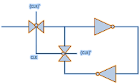
A D-latch is composed of two inverters, connected in positive feedback loop which is tristated when input data path is enabled. On the other hand, when data path is tristated, this loop is enable
A D-type latch

Cause/origin of setup time and hold timeSetup time and hold time are said to be the backbone of timing analysis. Rightly so, for the chip to function properly, setup and hold timing constraints need to be met properly for each and every flip-flop in the design. If even a single flop exists that does not meet setup and hold requirements for timing paths starting from/ending at it, the design will fail and meta-stability will occur. It is very important to understand the origin of setup time and hold time as whole design functionality is ensured by these. Let us discuss the origin of setup time and hold time taking an example of D-flip-flop as in VLSI designs, D-type flip-flops are almost always used. A D-type flip-flop is realized using two D-type latches; one of them is positive level-sensitive, the other is negative level-sensitive. A D-type latch, in turn, is realized using transmission gates and inverters. Figure below shows a positive-level sensitive D-type latch. Just inverting the transmission gates’ clock, we get negative-level sensitive D-type latch.

A complete D flip-flop using the above structure of D-type latch is shown in figure below:

 A D-type flip-flop consists of two latches connected back to back in master-slave format
A D-type flip-flop


Now, let us get into the details of above figure. For data to be latched by ‘latch 1’ at the falling edge of the clock, it must be present at ‘Node F’ at that time. Since, data has to travel ‘NodeA’ -> ‘Node B’ -> ‘Node C’ -> ‘Node D’ -> ‘Node E’ -> ‘Node F’ to reach ‘Node F’, it should arrive at flip-flop’s input (Node A) at some earlier time. This time for data to reach from ‘Node A’ to ‘Node F’ is termed as data setup time (assuming CLK and CLK' are present instantaneously. If that is not the case, it will be accounted for accordingly). Similarly, it is necessary to ensure a stable value at the input to ensure a stable value at ‘Node C’. In other words, hold time can be termed as delay taken by data from ‘Node A’ to ‘Node C’.

Setup and hold checks in a design: Basically, setup and hold timing checks ensure that a data launched from one flop is captured at another properly. Considering the way digital designs of today are designed (finite state machines), the next state is derived from its previous state.  So, data launched at one edge should be captured at next active clock edge. Also, the data launched from one flop should not be captured at next flop at the same edge. These conditions are ensured by setup and hold checks. Setup check ensures that the data is stable before the setup requirement of next active clock edge at the next flop so that next state is reached. Similarly, hold check ensures that data is stable until the hold requirement for the next flop for same clock edge has been met so that present state is not corrupted.

A timing path from rise edge-triggered flip-flop to rise edge-triggered flip-flop
A sample path in a design
Shown above is a flop-to-flop timing path. For simplicity, we have assumed that both the flops are rise edge triggered. The setup and hold timing relations for the data at input of second flop can be explained using the waveforms below:


waveform showing setup and hold requirement for the sample timing path shown above
Figure showing setup and hold checks being applied for the timing path shown above


As shown, data launched from launching flop is allowed to arrive at the input of the second flop only after a delay greater than its hold requirement so that it is properly captured. Similarly, it must not have a delay greater than (clock period – setup requirement of second flop). In other words, mathematically speaking, setup check equation is given as below (assuming zero skew between launch and capture clocks):
                                Tck->q + Tprop + Tsetup < Tperiod
 Similarly, hold check equation is given as:
                               Tck->q  + Tprop > Thold

If we take into account skews between the two clocks, the above equations are modified accordingly. If Tskew is the skew between launch and capture flops, (equal to latency of clock at capture flop minus latency of clock at launch flop so that skew is positive if capture flop has larger latency and vice-versa), above equations are modified as below:
                    
                      Tck->q + Tprop + Tsetup - Tskew < Tperiod
                      Tck->q  + Tprop > Thold + Tskew

Setup checks and hold checks for reg-to-reg paths explains different cases covering setup and hold checks for flop-to-flop paths.

What if setup and/or hold violations occur in a design: As said earlier, setup and hold timings are to be met in order to ensure that data launched from one flop is captured properly at the next flop at next clock edge so as to transfer the state-machine of the design to the next state. If the setup check is violated, the data will not be captured at the next clock edge properly. Similarly, if hold check is violated, data intended to be captured at the next edge will get captured at the same edge. Setup hold violations can also lead to data changing within setup/hold window of the capturing flip-flop. It may lead to metastability failure in the design (as explained in our post 'metastability'). So, it is necessary to have setup and hold requirements met for all the flip-flops in the design and there should not be any setup/hold violation.
What if you fabricate a design without taking care of setup/hold violations: If you fabricate a design having setup violations, you can still use it by lowering the frequency as the equation involves the variable clock frequency. On the other hand, a design with hold violation cannot be run properly. So, if you fabricate a design with an accidental hold violation, you will have to simply throw away the chip (unless the hold path is half cycle as explained here). A design with half cycle hold violations only can still be used at lower frequencies.

Tackling setup time violation As given above, the equation for setup timing check is given as:
            Tck->q + Tprop + Tsetup - Tskew < Tperiod

The parameter that represents if there is a setup time violation is setup slack. The setup slack can be defined as the difference between the L.H.S and R.H.S. In other words, it is the margin that is available such that the timing path meets setup check. The setup slack equation can be given as:
            Setup slack = Tperiod -  (Tck->q + Tprop + Tsetup - Tskew)
If setup slack is positive, it means there is still some margin available in the timing path. On the other hand, a negative slack means that the paths violates setup timing check by the amount of setup slack. To get the path met, either data delay should be decreased or clock period should be increased.

Mitigating setup violation: Thus, we can meet the setup requirement, if violating, by 
1. Decreasing clk->q delay of launching flop 
2. Decreasing the propagation delay of the combinational cloud 
3. Reducing the setup time requirement of capturing flop 
4. Increasing the skew between capture and launch clocks
5. Increasing the clock period

Tackling hold time violation: Similarly, the equation for hold timing check is as below:
            Tck->q + Tprop > Thold + Tskew
The parameter that represents if there is a hold timing violation is hold slack. The hold slack is defined as the amount by which L.H.S is greater than R.H.S. In other words, it is the margin by which timing path meets the hold timing check. The equation for hold slack is given as:
            Hold slack = Tck->q + Tprop - Thold - Tskew
If hold slack is positive, it means there is still some margin available before it will start violating for hold. A negative hold slack means the path is violating hold timing check by the amount represented by hold slack. To get the path met, either data path delay should be increased, or clock skew/hold requirement of capturing flop should be decreased.

Mitigating hold violation: We can meet the hold requirement by:
  1. Increasing the clk->q delay of launching flop
  2. Decreasing the hold requirement of capturing flop
  3.  Decreasing clock skew between capturing clock and launching flip-flops
Also read:

Lockup latch – principle, application and timing

What are lock-up latches: Lock-up latch is an important element in scan-based designs, especially for hold timing closure of shift modes. Lock-up latches are necessary to avoid skew problems during shift phase of scan-based testing. A lock-up latch is nothing more than a transparent latch used intelligently in the places where clock skew is very large and meeting hold timing is a challenge due to large uncommon clock path. That is why, lockup latches are used to connect two flops in scan chain having excessive clock skews/uncommon clock paths as the probability of hold failure is high in such cases. For instances, the launching and capturing flops may belong to two different domains (as shown in figure below). Functionally, they might not be interacting. Hence, the clock of these two domains will not be balanced and will have large uncommon path. But in scan-shift mode, these interact shifting the data in and out. Had there been no lockup latches, it would have been very difficult for STA engineer to close timing in a scan chain across domains. Also, probability of chip failure would have been high as there a large uncommon path between the clocks of the two flops leading to large on-chip-variations. That is why; lockup latches can be referred as as the soul mate of scan-based designs.

Lockup latches are needed where there is need to fix hold due to large skew between clock signals for launch and capture flops

Figure 1 : Lockup latches - the soul mate of scan-based designs


Where to use a lock-up latch: As mentioned above, a lock-up latch is used where there is high probability of hold failure in scan-shift modes. So, possible scenarios where lockup latches are to be inserted are:

  • Scan chains from different clock domains: In this case, since, the two domains do not interact functionally, so both the clock skew and uncommon clock path will be large.
  • Flops within same domain, but at remote places: Flops within a scan chain which are at remote places are likely to have more uncommon clock path. 
In both the above mentioned cases, there is a great chance that the skew between the launch and capture clocks will be high. There is both the probability of launch and capture clocks having greater latency. If the capture clock has greater latency than launch clock, then the hold check will be as shown in timing diagram in figure 3. If the skew difference is large, it will be a tough task to meet the hold timing without lockup latches.

A timing path crossing from one domain to another

Figure 2: A path crossing from domain 1 to domain 2 (scope for a lock-up latch insertion)

Waveform showing the skew between launch and capture clocks, resulting in hold violation

Figure 3: Timing diagram showing setup and hold checks for path crossing from domain 1 to domain 2

Positive or negative level latch?? It depends on the path you are inserting a lock-up latch. Since, lock-up latches are inserted for hold timing; these are not needed where the path starts at a positive edge-triggered flop and ends at a negative edge-triggered flop. It is to be noted that you will never find scan paths originating at positive edge-triggered flop and ending at negative edge-triggered flop due to DFT specific reasons. Similarly, these are not needed where path starts at a negative edge-triggered flop and ends at a positive edge-triggered flop. For rest two kinds of flop-to-flop paths, lockup latches are required. The polarity of the lockup latch needs to be such that it remains open during the inactive phase of the clock. Hence,

  • For flops triggering on positive edge of the clock, you need to have latch transparent when clock is low (negative level-sensitive lockup latch)
  • For flops triggering on negative edge of the clock, you need to have latch transparent when clock is high (positive level-sensitive lockup latch)
Who inserts a lock-up latch: These days, tools exist that automatically add lockup latches where a scan chain is crossing domains. However, for cases where a lockup latch is to be inserted in an intra-domain scan chain (i.e. for flops having uncommon path), it has to be inserted during physical implementation itself as physical information is not feasible during scan chain implementation (scan chain implementation is carried out at the synthesis stage itself).

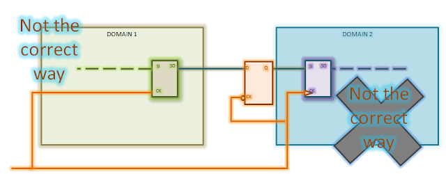
Which clock should be connected to lock-up latch: There are two possible ways in which we can connect the clock pin of the lockup latch inserted. It can either have same clock as launching flop or capturing flop. Connecting the clock pin of lockup latch to clock of capturing flop will not solve the problem as discussed below.
  •  Lock-up latch and capturing flop having the same clock (Will not solve the problem): In this case, the setup and hold checks will be as shown in figure 5. As is apparent from the waveforms, the hold check between domain1 flop and lockup latch is still the same as it was between domain 1 flop and domain 2 flop before. So, this is not the correct way to insert lockup latch.


It is not appropriate to connect the capture flop's clock to the lockup latch as hold check will be the same

Figure 4: Lock-up latch clock pin connected to clock of capturing flop

Waveform showing the inability of connecting capture flop's clock in meeting hold

Figure 5: Timing diagrams for figure 4


  •  Lock-up latch and launching flop having the same clock: As shown in figure 7, connecting the lockup latch to launch flop’s clock causes the skew to reduce between the domain1 flop and lockup latch. This hold check can be easily met as both skew and uncommon clock path is low. The hold check between lockup latch and domain2 flop is already relaxed as it is half cycle check. So, we can say that the correct way to insert a lockup latch is to insert it closer to launching flop and connect the launch domain clock to its clock pin.

The correct way to connect the clock to lockup latch is to connect it with the clock coming at launch flop

Figure 6: Lock-up latch clock pin connected to clock of launch flop

Waveform for the connection of clock pin of lockup latch to launch flop's clock

Figure 7: Waveforms for figure 6


Why don’t we add buffers: If the clock skew is large at places, it will take a number of buffers to meet hold requirement. In normal scenario, the number of buffers will become so large that it will become a concern for power and area. Also, since skew/uncommon clock path is large, the variation due to OCV will be high. So, it is recommended to have a bigger margin for hold while signing it off for timing. Lock-up latch provides an area and power efficient solution for what a number of buffers together will not be able to achieve.

Advantages of inserting lockup latches:
  • Inserting lock-up latches helps in easier hold timing closure for scan-shift mode
  • Robust method of hold timing closure where uncommon path is high between launch and capture flops
  • Power efficient and area efficient
  • It improves yield as it enables the device to handle more variations.
Lockup registers: Instead of latches, registers can also be used as lockup elements; however, they have their own advantages and disadvantages. Please refer to Lockup latches vs. lockup registers : what to chose for a comparative study of using lockup latches vs lockup registers.

References:
1)  Why not add buffer but lockup latch” - http://www.edaboard.com/thread82364.html

Also read: