Clock multiplexer for glitch-free clock switching

In the post clock switching and clock gating checks, we discussed how important it is to have a glitch free clock. Also, in clock gating checks at a multiplexer, we discussed the conditions wherein a normal multiplexer can be used to propagate a clock without any glitches. 


In this post, we will discuss about multiplexer circuit for clock switching which can safely switch clocks without the probability of any glitches under most of the scenarios, hence, also called glitch-less multiplexer.


Definition of clock multiplexer: Let us first define a clock multiplexer "A clock multiplexer is a circuit that can switch the system from one clock to another while the chip is running. The two frequencies may be related to each other, or may to totally unrelated". A clock multiplexer switches the clock without any glitches as the glitch in clock will be hazardous for the system. Hence, a clock multiplexer is also known as a glitchless multiplexer.

Clock multiplexer for switching between two synchronous clocks:


Clock multiplexer for switching between two asynchronous clocks:


Reference: A very detailed and good explanation is provided at below link. I recommend to go through this for complete understanding of the process.
http://www.eetimes.com/document.asp?doc_id=1202359


Also read:

STA problem: Finding setup and hold slack taking into accoung clock skew

Problem: Figure 1 below shows a timing path from a positive edge-triggered flip-flop to a positive edge-triggered flip-flop. Considering clock frequency of 200 MHz, find the setup and hold slacks for this timing path.

Solution:


Figure 1: Timing path


As the clock frequency is given as a 200 MHz, time period = 1/frequency = 5 ns.

Let us first calculate the setup slack. The setup timing equation is given as:
Tck->q + Tprop + Tsetup - Tskew < Tperiod
And equation for setup slack is given as:
SS = Tperiod - (Tck->q + Tprop + Tsetup - Tskew)  
Here,
Tck->q = 2ns, Tprop (max value of delay of combinational logic) = 4 ns+ Tsetup = 1 ns,   Tperiod = 5 ns, Tskew = 1 ns
 Putting these values into equation for setup slack, we get setup slack for this timing path.

SS = 5 - (2 + 4 + 1 - 1) ns
SS = -1 ns

Now, hold slack can be found out from the hold timing equation. The hold timing equation is given as:
Tck->q  + Tprop > Thold + Tskew
Here,
Tck->q  =  2 ns, Tprop (min value of combinational propagation delay) = 4 ns, Thold = 1ns, Tskew = 1 ns
 And the equation for hold slack is given as:

HS = Tck->q  + Tprop  - (Thold + Tskew
HS = 2 + 4 - (1 + 1) = 4 ns 
So, for this timing path, setup slack value is -1 ns and hold slack value is 4 ns.

STA problem: Finding setup and hold slack considering ideal clock

Problem: Figure 1 below shows a timing path from a positive edge-triggered flip-flop to a positive edge-triggered flip-flop. Considering ideal clocks, and clock frequency of 100 MHz, find the setup and hold slacks for this timing path.

Solution:
Figure 1: Timing path


Ideally, all the flip-flops in design should get clock at the same time. So, ideal clock means that launch as well as capture flip-flops get clock at zero time. In other words, we can assume that clock skew is zero between start and end points.

As the clock frequency is given as a 100 MHz, time period = 1/frequency = 10 ns.

Let us first calculate the setup slack. The setup timing equation is given as:
Tck->q + Tprop + Tsetup - Tskew < Tperiod
And equation for setup slack is given as:
SS = Tperiod - (Tck->q + Tprop + Tsetup - Tskew)  
Here,
Tck->q = 2ns, Tprop (max value of delay of combinational logic) = 4 ns+ Tsetup = 1 ns,   Tperiod = 10 ns
 Putting these values into equation for setup slack, we get setup slack for this timing path.

SS = 10 - (2 + 4 + 1 - 0) ns
SS = 3 ns

Now, hold slack can be found out from the hold timing equation. The hold timing equation is given as:
Tck->q  + Tprop > Thold + Tskew
Here,
Tck->q  =  2 ns, Tprop (min value of combinational propagation delay) = 4 ns, Thold = 1 ns
 And the equation for hold slack is given as:

HS = Tck->q  + Tprop  - (Thold + Tskew
HS = 2 + 4 - (1 + 0) = 5 ns 
So, for this timing path, setup slack value is 3 ns and hold slack value is 5 ns.

LVS in VLSI

LVS stands for Layout vs Schematic. It is one of the steps of physical verification; the other one being DRC (Design Rule Check). While DRC only checks for certain layout rules to ensure the design will be manufactured reliably, functional correctness of the design is ensured by LVS.

Layout vs Schematic (LVS) compares the design layout with the design schematic/netlist to tell if the design is functionally equivalent to schematic. For this, the connections are extracted from layout of the design by using a set of rules to convert the layout to connections. These connections are, then compared if they match with the connections of the netlist. If the connections match, the LVS is said to be clean. 

VLSI - 2 ( Analog)

For those of you who wanted to make a career in analog, be a devotee of IIT Madras faculty irrespective of which IIT or which college you end up joining for your Mtech.

1. Shanti Pavan - IIT Madras videos
2. Nagendra Krishnapura - IIT Madras videos
3. Razavi - Videos and Text book
4. Anirudhan  - IIT Madras videos

I would like to discuss few common blunders, that we end up doing, which henceforth make us loose confidence in analog


Mistake 1 :  Two current sources in series

In simulation if you put two current sources in series and simulate this, you observe some crazy things happen, kindly do this and learn on this.


Put up a current source with NMOS sinking the current with very low Vgs and observe

Repeat the experiment with PMOS too. Try increasing the sizing for the same Vgs and observe what happens.

This experiments are really the most powerful in analog. The deeper one digs into this, the faster he understands the analog concepts well.

Spend great time dealing with this circuit.

Feel free to discuss if any doubts.......

Will come back with the next post. and discuss the solution and concepts here.

VLSI - 1


Without doubt, VLSI is top branch of ECE which fascinates many graduates and also a hot cake, henceforth making it a very competitive branch to get into even in your Mtech.

Roughly one can divide VLSI into 3 specializations:

Analog VLSI
Digital VLSI
Device Electronics


Analog VLSI  --- is something that really fascinates many VLSI students but often, doesn't become a career option for many of those bright students. It is much more than the coding stuff. Analog needs your thinking cap to be on always. It needs understanding of device physics too to a reasonable extent.

Any chip that gets taped out has all blocks of analog, digital. Band gap ckts, Reference current sources, IO components, PLLs, Amplifiers, filters, transmitters, receivers and many blocks are all analog in nature.

Most of the digital stuff are coded and even the interface circuits that is A/D convertors, sensors, and D/A convertors are all analog blocks !!!

The real world is analog in nature and any advancements we talk about DSP, can be appreciated only if u have proper interface circuits to convert the analog signal to digital and do DSP and convert it back to analog again.


Difference between fluorescence and phosphorescence

When electron beam hits phosphorus coated screen, some of the energy of these electrons in dissipated as heat and rest is transferred to electrons of phosphorus which makes them jump to higher energy levels. As we know that higher energy state is unstable and when electron comes to its original state energy is emitted in the form of light(color of light depend upon level from which electrons is returning).

In Ph, some energy levels are less stable than others so electrons in this state returns more rapidly than others.

 Hence energy(in the form of light) emitted when these unstable electron return from higher state to its original state while electrons are bombarded on it is called fluorescence.

While the  energy emitted when stable electrons return from higher energy levels to its original energy level once electron beam excitation is removed is called phosphorescence.

most of the light emitted in typical Ph is phosphorescence.

Persistence : It is defined as the time from removal of excitation of electron beam to the time when the phosphorescence has decayed to 10% of initial light output. Typically it is between 10-60 microsecond. 

How to fix hold violations

In the post setup and hold time violations, we learnt about the setup time violations and hold time violations. In this post, we will learn the approaches to tackle hold time violations. Following strategies can be useful in reducing the magnitude of hold violation and bringing the hold slack towards a positive value:

1. Insert delay elements: This is the simplest we can do, if we are to decrease the magnitude of a hold time violation. The increase in data path delay can be increased if we insert delay elements in the data-path. Thus, the hold violating path's delay can be increased, and hence, slack can be made positive by inserting buffers in hold violating data-path.

2. Reduce the drive strength of data-path logic gates: Replacing a cell with a similar cell of less drive strength will certainly add delay to data-path. However, there is a slight chance of decrease in data-path delay if the cell load is dominated by intrinsic capacitance as we discussed in how delay of a standard cell changes with drive strength

3. Use data-path cells with higher threshold voltages: If you have multiple flavors of threshold voltages in your design, the cells with higher threshold voltage will certainly have higher delays. So, this must be the first option you must be looking for to resolve hold violations.

4. Improve hold time of capturing flip-flop: Using a capturing flip-flop with higher drive strength and/or lower threshold voltage will give a lower hold time requirement. Also, improving the transition at flip-flop's clock pin reduces its hold time requirement.

5. Detoured routing: Detoured routing can be adoped as an alternative to insertion of delay elements as it will add load to the driving cell as well as provide additional net delay thereby increasing the data-path delay.

6. Play with clock skew: A positive skew degrades hold timing and a negative skew aids hold timing. So, if a data-path is violating, we can either decrease the latency of capturing flip-flop or increase the clock latency of launching flip-flop. However, in doing so, we need to keep in mind the setup and hold slacks of other timing paths starting and/or ending at these flip-flops.

7. Increase the clk->q delay of launching flip-flop: A launching flip-flop with more clk->q delay will help ease the hold timing of the data-path. For this, either we can decrease the drive strength of the flip-flop or move it to higher threshold voltage.

Also read:

How to fix setup violations

In the post setup and hold time violations, we learnt about the setup time violations and hold time violations. In this post, we will learn the approaches to tackle setup time violations. Following strategies can be useful in reducing the magnitude of setup violation and bringing it closer towards a positive value:

1. Increase the drive strength of data-path logic gates: A cell with better drive strength can charge the load capacitance quickly, resulting in lesser propagation delay. Also, the output transition should improve resulting in better delay of proceeding stages.
We can view a logic gate as a certain ON-resistance, that will charge/discharge a load capacitor to toggle the output state. This will form an RC circuit with a certain RC time constant. A better drive-strength gate will have a lesser resistance, effectively lowering the RC time constant; hence, providing less delay. This is illustrated in figure 1 below. If an AND gate of drive strength 'X' has a pull down resistance equivalent to 'R', the one with drive strength '2X' will have R/2 resistance. Thus, a bigger AND gate with better drive strength will have less delay.


This strategy is going to give best results only if the load of the cell is dominated by external load capacitance. Generally, drive strength of a cell is proportional to the cell size. Thus, increasing the cell size halves its internal resistance, but doubles the internal node capacitance. Thus, as shown in figure 2, the zero load capacitance delay of a cell ideally remains same of doubling the size of the cell.


Thus, upon doubling the drive strength of the cell, (assuming D to be the original delay) the delay can be anything between D/2 to D depending upon the ratio of intrinsic and external load capacitance.

Moreover, the input pin capacitance is a by-product of the size of the cell. Thus, increasing the size of the cell results in increased load for the driver cell of its input pins. So, in some cases (very high drive strength cell with less load driven by a low drive strength cell), increasing the drive strength can result in increase in magnitude of setup violation.

Keeping aside timing, power dissipation (both leakage as well as dynamic power) are a function of cell drive strength. Also, area is a function of cell drive strength. So, increasing the drive strength to fix a setup violation results in both area and power increase (although very small in comparison to whole design).


2. Use the data-path cells with lesser threshold voltages: If you have multiple flavors of threshold voltages in your designs, the cell with lesser threshold voltage will certainly have less delay. So, this must be the first step to resolve setup violations.


3. Improve the setup time of capturing flip-flop: As we know, the setup time of a flip-flop is a function of the transition at its data pin and clock pin. Better the transition at data pin, less is setup time. And worse clock transition causes less setup time. Also, a flip-flop with higher drive strength and/or lower threshold voltage is more probable of having less setup time requirement. Also, increasing the drive strength of flip-flop might cause the transition at clock pin and data pin to get worse due to higher pin loads. This also plays a role in deciding the setup time.

4. Restructuring of the data-path: Based upon the placement of data path logic cells, you can decide either to combine simple logic gates into a complex gate, or split a multi-stage cell into simpler logic gates. A multi-stage gate is optimized in terms of area, power and timing. For example, a 2:1 mux will have less logic delay than 1 AND gate and 1 OR gate combined for same output load capacitance. But, if you need to traverse distance, then 2 stages of logic can help as a buffer will introduce additional delay.
Let us elaborate this with the help of an example wherein a data-path traverses a 3-input AND gate from FF1 to FF2 situated around 400 micron apart. Let us assume one logic cell can drive 200 micron and each logic cell has only one drive strength available for simplicity. The choice is between two 2-input AND gates and 1 3-input AND gate. In this case, 3-input AND gate should give less delay (may be 200 ps for two 2-input AND vs 150 ps for one 3-input AND) as it has been optimized for less area, timing and power as compared to two 2-input AND gates.


Now, consider another case where the FF1 and FF2 are at a distance of 600 micron. In this case, if we use two 2-input AND gates, we can place them spaced apart 200 micron and hence, can cover the distance. But, if we use one 3-input AND gate, we will need to add a repeater, which will have its own delay. In this case, using two 2-input AND gates should give better results in terms of overall data-path delay.
 

5. Routing topologies: Sometimes, when there are a lot of nets at a certain place in the design, the routing tool can detour the nets trying to get the place less congested. Thus, two logic cells might be placed very close, still the delay can seem to be high for both the cells ; for driver cell due to high net capacitance and for load cell due to poor transition at the input. Also, net delay can be a significant component in such scenarios. Below figure shows one such example of two AND gates situated a certain distance apart. Ideally, there could be a straight net route between the two gates. But, due to very high net density in the region, router tool chose to route the way as shown on the right to help ease the congestion (this is an exaggerated scenario to help understand better).

So, always give proper importance to net routing topology, at least for setup timing critical nets. A few tips to improve the timing you can try include:

  • Try the net to have as less detouring as possible
  • Vias increase the net resistance. So, try to have as less vias as possible
  • Higher metal layers have less resistance. So, long nets can be routed in higher layers to have less net delay

6. Add repeaters: Every logic cell has a limit upto which it can drive a load capacitance. After that, its delay starts increasing rapidly. Since, net capacitance is a function of net length, we should keep a limit on the length of net driven by a gate. Also, net delay itself is proportional to square of net length. Moreover, the transitions may be very bad in such cases. So, it is wise to add repeater buffers after a certain distance, in order to ensure that the signal is transferred reliably, and in time.

7. Play with clock skew: Positive skew helps improve the setup slack. So, to fix setup violation, we may either choose to increase the clock latency of capturing flip-flop, or decrease the clock latency of launching flip-flop. However, in doing so, we need to be careful regarding setup and hold slack of other timing paths that are being formed from/to these flip-flops.

8. Increase clock period: As a last resort, you may choose to time your design at reduced frequency. But, if you are targeting a particular performance, you need a minimum frequency. In that case, this option is not for you.

9. Improve the clk->q delay of launching flip-flop: A flip-flop with less clk->q delay will help meeting a violating setup timing path. This can be achieved by:
  • Improving transition at flip-flops clock pin
  • Choosing a flip-flop of high drive strength. However, if by doing so, clock transition degrades, delay can actually increase
  • Replacing the flip-flop with a flip-flop of same drive strength, but lower Vt
In this post, we learnt how to approach a setup violating timing path. Have you ever used a method that is not listed above? Please share your experience in comments. We will be happy to hear from you.

Also read:

Setup and hold violations

What is meant by setup and/or hold violations: The ultimate aim of timing analysis is to get the design work at required frequency and with reliability. For this to happen, it must be ensured in timing that all the state transitions are happening smoothly; i.e., the setup and hold requirements of all the timing paths in the design are met. If there are failing setup and/or hold paths, the design is said to have violations.

What if setup and/or hold violations occur in a design: As said earlier, setup and hold timings are to be met in order to ensure that data launched from one flop is captured properly at another and in accordance to the state machine designed. In other words, no timing violations means that the data launched by one flip-flop at one clock edge is getting captured by another flip-flop at the desired clock edge. If the setup check is violated, data will not be captured properly at the next clock edge. Similarly, if hold check is violated, data intended to get captured at the next edge will get captured at the same edge. Moreover, setup/hold violations can lead to data getting captured within the setup/hold window which can lead to metastability of the capturing flip-flop (as explained in our post metastability). So, it is very important to have setup and hold requirements met for all the registers in the design and there should not be any setup/hold violations.

Setup violations: As we know, setup checks are applied for timing paths to get the state machine to move to the next state. The timing equation for a setup check from positive edge-triggered flip-flop to positive edge-triggered flip-flop is given as below:
                       Tck->q + Tprop + Tsetup - Tskew < Tperiod
For a timing path to meet setup requirements, this equation needs to be satisfied. The difference between left and right sides is represented by a parameter known as setup slack.

Setup slack is the margin by which a timing path meets setup check requirement. It is given as the difference in R.H.S. and L.H.S. of setup timing equation. The equation for setup slack is given as:
                        Setup slack = Tperiod -  Tck->q - Tprop - Tsetup + Tskew
If setup slack is positive, it means the timing path meets setup requirement. On the other hand, a negative setup slack means setup violating timing path. If, by chance, a fabricated design is found to have a setup violation, you can still run the design at less frequency than specified and get the desired functionality as setup equation includes clock period as a variable.

If we analyze setup equation more closely, it involves four parameters:
  1. Data path delay: More the total delay of data path (flip-flop delay + combinational delay + Setup), less is setup slack
  2. Clock skew: More the clock skew (difference between arrival times of clock at capture and launch flip-flops), more is the setup slack
  3. Setup time requirement of capturing flip-flp: Less the setup time requirement, more will be setup slack
  4. Clock period: More is the clock period, more is the setup slack. However, if you are targetting a specific clock period, doing this is not an option. :-)
How to tackle setup violations: The ultimate goal of timing analysis is to get every timing path follow setup equation and get a positive setup slack number for every timing path in the design. If a timing path is violating setup timing (assuming we are targetting a certain clock frequency), we can try one or more of the following to bring the setup slack back to a positive value by:
  • Decreasing data path delay
  • Choosing a flip-flop with less setup time requirement
  • Increasing clock skew
How to fix setup violations discusses various ways to tackle setup violations.

Hold violations: As we know, hold checks are applied to ensure that the state machine remains in its present state until desired. The hold timing equation for a timing path from a positive edge-triggered flip-flop to another positive edge-triggered flip-flop is governed by the following equation:
               Tck->q + Tprop > Thold + Tskew
Similar to setup slack, the presence and magnitude of hold violation is governed by a parameter called as hold slack. The hold slack is defined as the amount by which L.H.S is greater than R.H.S. In other words, it is the margin by which timing path meets the hold timing check. The equation for hold slack is given as:
Hold slack = Tck->q + Tprop - Thold + Tskew
If hold slack is positive, it means there is still some margin available before it will start violating for hold. A negative hold slack means the path is violating hold timing check by the amount represented by hold slack. To get the path met, either data path delay should be increased, or clock skew/hold requirement of capturing flop should be decreased.

If we analyze hold timing equation more closely, it involves three parameters:
  1. Data path delay: More data path delay favours hold slack; hence, more data path delay, more is the margin
  2. Skew: Having a positive skew degrades hold slack
  3. Hold requirement of capturing flip-flop: Less the hold requirement, more will be hold slack
How to tackle hold violations: Similar to setup analysis, the ultimate aim of hold analysis is to get every timing path follow the hold timing equation and get a positive hold slack for each and every timing path in the design. If a timing path violates for hold, we can do either of the following:
  • Increase data path delay
  • Decrease clock skew
  • Choose a flip-flop with less hold requirement

VHDL


Listing below the posts related to VHDL and HDL coding. Please provide your feedback in comments as to what more posts you wish to see here:

Clock skew


Clock skew is one of the most important parameters of a good physical design implementation. Keeping the clock skew to a minimum is considered to be a good measure of clock tree synthesis. 

Definition of clock skew: Clock skew between two flip-flops represents the difference in arrival times of clock signal at the respective clock pins. If there is a timing path being formed between the two flip-flops, then we can attribute a sign to the clock skew. In that case, clock skew is given as:
Clock skew = (Arrival time at capture clock pin) - (Arrival time at launch clock pin)
Thus, based upon the sign of clock skew, we get two types of clock skew labelled as positive skew and negative skew.

Positive clock skew: If the clock arrival time at capture flip-flop is greater than that at launch flip-flop, clock skew is said to be positive. Assuming all buffers take the same delay, figure 1 shows a scenario of positive clock skew.


As shown in figure 1 above for the case of positive clock skew, flip-flop capturing data is getting delayed clock signal. So, the data that is launched gets additional time before it is captured at the next edge. So, setup check gets relaxed by the amount equivalent to clock skew. On the other hand, for hold check, the data has to be kept stable for an extra amount of time equal to the clock skew. So, hold check gets tightened in case clock skew is positive. The same is shown in figure 2 below.


Negative clock skew: Contrary to positive clock skew, if the clock arrival time at capture flip-flop is less than the launch flip-flop, clock skew is said to be negative. Figure 3 shows a scenario of negative clock skew as the launch flip-flop getting a delayed version of clock signal.


Since, the launching flip-flop is getting a delayed version of clock, the data launched gets less than one clock period to travel to the capturing flip-flop. So, negative clock skew makes setup check tighter by the magnitude of clock skew. On the other hand, for hold check, data has to be stable for less time after the arrival of clock edge. In other words, hold check gets relaxed by the same amount. Figure 4 below shows the scenario of negative clock skew.


What makes timing paths both setup critical and hold critical

Those timing paths, which are very hard to meet in timing are called timing critical paths. They can be divided into setup and hold timing critical paths.

Setup timing critical paths: Those paths for which meeting setup timing is difficult, can be termed as setup critical timing paths. For these paths, the setup slack value is very close to zero and for the most part of design cycle, remains below zero.

Hold timing critical paths: As is quite obvious, those paths for which meeting hold timing is difficult, are hold critical paths. These paths may require many buffers to meet hold slack equation.

Sometimes, we may encounter some timing paths which are violating in both setup and hold. There is not enough setup slack to make them hold timing clean and vice-versa. The good practice in timing analysis is to identify all such paths as early as possible in design cycle. Let us discuss the scenarios that make timing paths both setup and hold timing critical.

Inherent frequency limit and delay variations: Let us say, we want our chip to remain functional within following PVTs:
Process : Best-case to Worst-case
Voltage : 1.2 V with 10% voltage variation allowed (1.08 V to 1.32 V)
Temperature : -20 degrees to +150 degress
The delay of a standard cell changes with PVTs and OCVs. Let us only talk about PVT variations. Let us say, cell delay changes by 2 times from worst case scenario (worst process, lowest voltage, worst temperature) to best case scenario (best process, highest voltage, best temperature). Let us say, setup and hold checks also scale by same amount. Remember that the equations for setup and hold need to be satisfied across all the PVTs.  Which essentially means setup needs to be ensured for WCS scenario and hold timing needs to be ensured for BCS scenario. This will provide a limit to maximum frequency that the path can be timed at. If we try to go beyond that frequency, we will not be able to ensure both setup and hold slacks remain positive.

Let us illustrate with the help of an example of a timing path from a positive edge-triggered flip-flop to positive edge-triggered flip-flop with a frequency target of 1.4 GHz (clock time period = 714 ps). Let us say, we have the Best-case and Worst-case scenarios as shown in figure 1 and 2.


Figure 1 shows that the best-case clk->q delay for launch flop is 100 ps, best-case combinational delay is 80 ps and best-case hold time is 200 ps. Applying our hold timing equation for this case,

Hold slack = Tck->q  + Tprop - Thold
Hold slack = 100 + 80 - 200
Hold slack = -20 ps
So, in this case, our hold slack comes out to be negative. So, we need to apply the techniques to improve our hold slack. But we need to ensure that our setup slack is sufficiently positive. Let us look at the worst-case scenario to know about our setup slack. If we assume that everything scales by 2 times, the worst-case numbers for clk->q delay, combinational delay and setup/hold time come out to be 200 ps, 160 ps and 400 ps respectively.


Applying setup timing equation for this scenario,
Setup slack = Tperiod - (Tck->q + Tprop + Tsetup)
Setup slack = 714 - 200 - 160 - 400 = -36 ps 

Thus, for the same timing path, both setup and hold slacks are coming out to be negative. For this path, we cannot meet both setup and hold provided all these conditions. One of the solutions could be to use cells with less delay variability. Or we can limit the operating conditions to a tighter range, for instance, 1.15 to 1.25 V instead. This will improve both setup and hold slack values. If this is not an option, the only option left to satisfy timing is to add delay elements to bring hold slack to zero and reduce the frequency as the inherent variations of cells will not allow the path to operate beyond a certain frequency. Let us check at what maximum frequency our timing path will work.

First, we need to ensure hold timing is met. Thus, 
Hold slack >= 0
This translates to Combinational delay (Cb) > 100 ps, or Cb = 100 ps for a hold slack of 0 ps. In other words, worst case combinational delay is 200 ps (2 times scaling).

For a setup slack of 0 ps, operating clock frequency will be maximum; i.e.,

Tperiod(min) = Tck->q + Tprop + Tsetup
Tperiod(min) = 200+ 200 + 400 = 800 ps 
The minimum time period that it can operate at is 800 ps, or a maximum frequency of 1.25 GHz.

In this post, we have discussed how PVT variations in delay can cause a timing path to be both setup and hold critical. Also, we discussed how it limits the frequency of operation. Although the discussion was limited to only PVT variations, OCV variations will add to the variations. The inherent equations will certainly remain same though. Also, we did not take an important parameter into consideration; i.e. clock skew. Can you think of how clock skew between the two flip-flops contribute to maximum achievable clock frequency? Or is it unrelated to clock skew?


Also read:


Fake currency!!

Problem: A woman goes to buy a pair of shoes. She stops at a shoe store and buys a pair of shoe worth 200 rupees. She hands a thousand rupee note to the shopkeeper. Shopkeeper is short of change, he goes to a nearby tea stall and brings the change. He keeps 200 rupees with himself, handing 800 rupees to the woman. After woman leaves, tea stall owner comes to the shoe store and claims the note to be a fake one. Shoe store owner checks it and agrees. Now the question is, who is in loss and by what amount?

Will post the solution to this puzzle after some time. Till then, let us know your thoughts.

Setup and hold checks

Setup and hold checks ensure that the finite state machine works in the way as designed. In essence, whole of the timing analysis, be it static or dynamic, revolves around setup and hold checks only. In this post, we will be touching upon setup and hold checks.

What is meant by setup check: Setup check ensures that the design transitions to the next state as desired through the state machine design. Mostly, the setup check is at next active clock edge relative to the edge at which data is launched. Let us call this as default setup check. This is, of course, in correspondence to state machine requirement to transfer to next state and the possibility of meeting both setup and hold checks together in view of delay variations accross timing corners. Figure 1 below shows the setup check for a timing path from positive edge-triggered register to negative edge-triggered register. It shows that the data launched by flop1 on positive edge will be captured by flop2 on the forthcoming negative edge and will update the state of flop2. To do so, it has to be stable at the input of flop2 before the negative edge at least setup time before.


Default setup check for positive edge-triggered register to negative edge-triggered register timing path
Figure 1: Default setup check for a timing path from positive edge-triggered to negative edge-triggered flop


What is meant by hold check: Hold check ensures that the design does not move to the next state before its stipulated time; i.e., the design retains its present state only. The hold check should be one active edge prior to the one at which setup is checked unless there are some architectural care-abouts in the state machine design. The hold check corresponding to default setup check in such a scenario is termed as default hold check. Of course, there are some architectural care-abouts for this to happen. Figure 2 below shows the default hold check corresponding to the default setup check of figure 1. It shows that the data launched on positive edge by flop 1 should be captured by next negative edge and not the previous negative edge.


Default hold timing check for a timing path from positive edge-triggered flip-flop to negative edge-triggered flip-flop
Figure 2: Default hold check for a timing path from positive edge-triggered


Default setup and hold check categories: As discussed above, for each kind of timing path, there is a default setup check and a default hold check that will be inferred unless there is an intended non-default check. We can split the setup and hold checks into following categories for our convenience. Each of the following is a link, which you can visit to know about the default setup and hold checks for each category:


Non-default setup and hold checks: These are formed when the state machine behavior is different than the default intended one. Sometimes, a state machine can be designed causing the setup and hold checks to be non-default. For this to happen, of course, you have to first analyze delay variations across timing corners and ensure that the setup timing equation and hold timing equation are satisfied for all timing corner scenarios. The non-default setup and hold checks can be modeled with the help of multi-cycle path timing constraints. You may wish to go through our posts Multicycle paths - the architectural perspective and Multicycle paths handling in STA to understand some of the concepts related to non-default setup and hold checks.

Positive, negative and zero setup time


As we know from the definition of setup time, setup time is a point on time axis which restrains data from changing after it. Data can change only before occurrence of setup timing point. Theoretically, there is no constraint on occurrence of setup time point with respect to clock active edge. It can either be before, after or at the same time as that of clock edge. Depending upon the relative occurrence of setup time point and clock active edge, setup time is said to be positive, zero or negative.

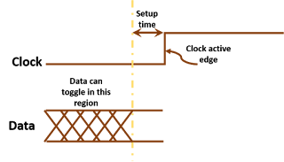
Positive setup time: When setup time point is  before the arrival of clock edge, setup time is said to be positive. Figure 1 below shows positive setup time.
When setup time point is  before the arrival of clock edge, setup time is said to be positive.
Figure 1: Positive setup time


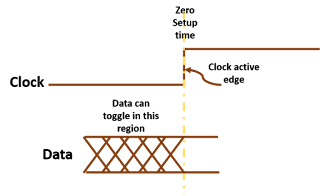
Zero setup time: When setup time point is at the same instant as clock's active edge, setup time is said to be zero. Figure 2 shows a situation wherein setup time is zero.

When setup time point is at the same instant as clock's active edge, setup time is said to be zero.
Figure 2: Zero setup time


Negative setup time: When setup time point occurs after clock edge, setup time is said to be negative. Figure 3 shows timing waveform for negative setup time.
When setup time point occurs after clock edge, setup time is said to be negative.
Figure 3: Negative setup time


What causes different values of setup time: We have discussed above theoretical aspects of positive, zero and negative setup time. Let us go a bit deeper into the details. Figure 4 shows a positive level-sensitive D-latch. As we know from the definition of setup time, setup time depends upon the relative arrival times of data and clock at input transmission gate (We have to ensure data has reached upto NodeD when clock reaches input transmission gate). Depending upon the relative arrival times of data and clock, setup time can be positive, zero or negative.
Figure 4: Positive level-sensitive latch
Let us assume the delay of an inverter is 1 ns. Then, to ensure that the data has reached NodeD when clock edge arrives at input transmission gate, data has to be available at the input transmission gate at least 2 ns before. So, if both data and clock reach the reference point at the same time, the latch has a setup time of 2 ns.

Now, if data takes 1 ns more than clock to reach input transmission gate from the reference point, then, data has to reach reference point at least 3 ns before clock reference point. In this case, setup time will be 3 ns.

Similarly, if data takes 1 ns less than clock to reach input transmission gate, setup time will be 1 ns. And if data takes 2 ns less than clock to reach input transmission gate, setup time will be zero.

Now, if there is further difference between delays of data and clock from respective reference points to input transmission gate, the hold time will become negative. For example, if data takes 3 ns less than clock to reach input transmission gate, setup time will be -1 ns.

This is how setup time depends upon relative delays of data and clock within the sequential element. And it completely makes sense to have negative setup time.

Also read:

Positive, negative and zero hold time


As we know from the definition of hold time, hold time is a point on time axis which restrains data from changing before it. Data can change only after hold time has elapsed. Now, there is no constraint on the occurrence of hold time point with respect to clock edge. It can either be after, before or at the same instant of time as that of clock active edge.

Posotive hold time: When hold time point is after the arrival of clock active edge, hold time is said to be positive hold time. Figure 1 below shows positive hold time.

Positive hold time, hold time, data can toggle after clock edge, data needs to be stable at least for hold time after clock edge
Figure 1: Positive hold time


Zero hold time: When hold time point is at the same time instant as that of clock active edge, we say that hold time of the sequential element is zero. Figure 2 below shows timing waveform for zero hold time.


Data can toggle right after clock edge
Figure 2: Zero hold time


Negative hold time: Similarly, when hold time point comes earlier on time scale as compared to data, we say that hold time of the sequential element is negative. Figure 3 shows timing waveform for negative hold time.

Negative hold time allows data to toggle even before clock ege
Figure 3: Negative hold time


We have discussed above theoretical aspects of positive, zero and negative hold time. Let us go a bit deeper into the details. Figure 4 shows a positive level-sensitive D-latch. As we know (from definition of hold time), hold time depends upon the relative arrival times of clock and data at the input transmission gate (We have to ensure data does not reach NodeC). Depending upon the times of arrival of clock and data, hold time can be positive or negative.

Figure 4: Positive level-sensitive D-latch

Let us say, the delay of an inverter is 1 ns. Then, we can afford the data to reach transmission gate input even 0.9 ns before arrival of clock at transmission gate. This will ensure data reaches NodeC (-0.9 + 1 =) 0.1 n after arrival of clock edge, if allowed. But, since, clock closes transmission gate, data will not reach NodeC. So, in this case, hold time is -1 ns. If the delay from NodeB to NodeC was something else, hold time would also have been different.

Now, if we say that clock arrives at transmission gate 1 ns earlier than data, then, by above logic, hold time of this latch will be -2 ns.

Similarly, if clock arrives at transmission gate 0.5 ns after data, hold time will be -0.5 ns.

And if clock arrive at transmission gate 1 ns after data, hold time will be  zero.

If the arrival time of clock is made more late, hold time will be greater than zero. For example, if arrival time of clock is 2 ns after data, hold time will be +1 ns.


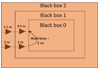
Hold time of the circuit is also dependent upon the reference point. For example, consider a multi-level black box as shown in figure 5. If we look at black box 0, its hold time is -1 ns. At level of black box 1, wherein clock travels 2 ns and data travels 0.5 ns to reach black box 0, hold time is (-1 + 2 - 0.5 = ) 0.5 ns. Similarly, at the level of black box 2, hold time is 1 ns. This is how, hold time depends upon the relative arrival times of clock and data. And it completely makes sense to have a negative hold time.

DFT basics

DFT stands for Design For Testification. DFT engineers try to make the testing of design more cost effective by introducing some structures into the design itself. By doing so, the overall test cost, and hence, cost of production comes down. Below, we list some of our posts covering the basics of DFT. Please provide your feedbacks regarding the topics you want to see as a part of this list. :-) Happy learning.