STA problem: Maximum frequency of operation of a timing path

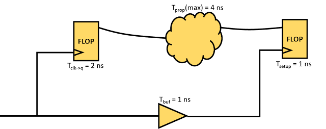
Problem: Figure 1 below shows a timing path from a positive edge-triggered register to a positive edge-triggered register. Can you figure out the maximum frequency of operation for this path?
find out the maximum frequency of operation for path shown
Figure 1: A sample timing path
Solution:
The above timing path is a single cycle timing path. The maximum frequency is governed by setup timing equation. In other words, maximum frequency of operation is the maximum frequency (minimum time period of clock) that satisfies the following condition:

 Tck->q + Tprop + Tsetup - Tskew < Tperiod
Here,
 Tck->q = 2 ns, Tprop = 4 ns, Tsetup = 1 ns, Tskew = 1 ns, Tperiod 
Now,
Tperiod > 2 ns + 4 ns + 1 ns - 1 ns
Tperiod > 6 ns
So, the minimum time period of the clock required is 6 ns. And the maximum frequency that the above circuit can work is (1000/6) MHz = 166.67 MHz.

It should be noted that at if we operate this timing path at maximum frequency calculated, setup slack will be zero. :-)

In this post, we talked about frequency of operation of single cycle timing paths. Can you figure out maximum frequency of operation for half cycle timing paths? Also, there is a relation of maximum operating frequency to hold timing? Can you think about this situation?

Also read:

Design Quiz: multiply by 2 clock circuit

Design problem: Make a simple circuit whose output clock is twice in frequency to the input clock.


An XOR gate with one of its input getting delayed version of the other input can act as a frequency multiplier. Since, an XOR gate produces a ‘0’ when both inputs are same, and ‘1’ when both inputs are different; if it gets delayed version of one input at the other, every time input toggles, a pulse is produced at the output. The duration of the pulse is equal to the delay introduced by delay element. The circuit and the resulting waveform is shown in figure 1 below. This circuit arrangement is also known as pulse generator as it produces a pulse on every toggle of input.


An XOR pulse generator circuit can act as a multiply by two, but it does not guarantee a duty cycle
(a) Multiply-by-2 clock circuit                                      (b) Input and output clock waveforms of multiply-by-2                                                                                                 clock circuit


Characteristics of XOR multiply by 2:
  • The output pulse duration is equal to the delay introduced by delay element.
  • For duty cycle to be equal to 50%, the delay element’s delay must be half that of input clock. Since, this cannot be guaranteed, the output duty cycle will not be 50%.
  • The delay element’s delay must be less than half the input clock period; otherwise it will not work
  • The inactive state of XOR multiply-by-2 will be 0 as it produces a '0' when both inputs are same. To implement a multiply-by-2 circuit with '1' as inactive state, you will have to use an XNOR gate.

Hope you’ve found this post useful. Let us know what you think in the comments.

Also read: