Reset basics

Purpose of reset: We see that almost every electronic device has a reset button. Your video game has a reset button that resets the game and your unsaved progress is lost. Your laptop's reset button reboots it. Have you ever wondered why a system (or specifically a chip) has a reset? Well, the simple purpose of resets is to provide a known initial state to the system to start with. Another reason is, when the system accidentally goes into some unknown state (there may be many reasons for this), the system always knows how to get out of this and go into a known state by asserting a reset signal. 

Reset design strategies: Defining a reset is one of the most important decisions that needs to be taken for the good health of design. In general, following things need to be kept in mind during deciding reset strategy:

  • What flops to receive reset: One of the easiest and safest approaches is to enable all the flip-flops in the design with a reset. However, there may be a some registers, whose initial state will not have any impact on the design state. In other words, it might not matter if the register's output is '0' or '1' when design goes in reset state. Such registers can be kept non-resettable after an analysis. Let us elaborate with the help of an example. Figure 1 shows a part of an FSM wherein two registers are feeding an AND gate. In figure 1(a), we have decided to initialize both to '0' during reset (with an asynchronous reset, to be explained later). However, given this scenario, if one of the flip-flops is provided with an initial state of '0', the output of the other will be gated. So, we may omit reset on one of the flip-flops. Figure 1(b) shows that omission of reset on one of the flip-flops does not have any impact on state machine design.


We may not always encounter such scenarios. If, instead of AND gate, we had an OR gate, we would not have been able to keep one of the flip-flops uninitialized during reset. Figure 2 shows such an example. In figure 2(b), if we remove reset from second flip-flop, output of OR gate goes 'X'; thus, impacting the state machine.


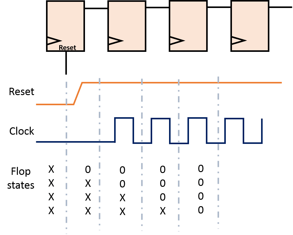
Another popular scenario wherein we can skip a few registers from having a reset pin is shift registers. If the first stage of a shift register is you give more than one clock pulses when in reset state, subsequent stages will get reset. If you have four stages, you need to give at least three clock pulses while in reset. The same is shown in figure below.

  • Synchronous vs asynchronous reset: There are two kinds of reset assertion/deassertion strategies - synchronous vs asynchronous reset. Although each of the two can be used to effective implementation of reset, each of these has its own advantages/disadvantages. Designer may decide upon the desired strategy by considering the pros and cons.
    • Synchronous reset means that the reset will affect the state of the design only on the active edge of the clock.
    • Asynchronous reset resets the design asynchronously. For this purpose, flip-flops have a special pin that resets the output to '0' or '1' based upon the need. 

Clock multiplexer for glitch-free clock switching

In the post clock switching and clock gating checks, we discussed how important it is to have a glitch free clock. Also, in clock gating checks at a multiplexer, we discussed the conditions wherein a normal multiplexer can be used to propagate a clock without any glitches. 


In this post, we will discuss about multiplexer circuit for clock switching which can safely switch clocks without the probability of any glitches under most of the scenarios, hence, also called glitch-less multiplexer.


Definition of clock multiplexer: Let us first define a clock multiplexer "A clock multiplexer is a circuit that can switch the system from one clock to another while the chip is running. The two frequencies may be related to each other, or may to totally unrelated". A clock multiplexer switches the clock without any glitches as the glitch in clock will be hazardous for the system. Hence, a clock multiplexer is also known as a glitchless multiplexer.

Clock multiplexer for switching between two synchronous clocks:


Clock multiplexer for switching between two asynchronous clocks:


Reference: A very detailed and good explanation is provided at below link. I recommend to go through this for complete understanding of the process.
http://www.eetimes.com/document.asp?doc_id=1202359


Also read:

STA problem: Finding setup and hold slack taking into accoung clock skew

Problem: Figure 1 below shows a timing path from a positive edge-triggered flip-flop to a positive edge-triggered flip-flop. Considering clock frequency of 200 MHz, find the setup and hold slacks for this timing path.

Solution:


Figure 1: Timing path


As the clock frequency is given as a 200 MHz, time period = 1/frequency = 5 ns.

Let us first calculate the setup slack. The setup timing equation is given as:
Tck->q + Tprop + Tsetup - Tskew < Tperiod
And equation for setup slack is given as:
SS = Tperiod - (Tck->q + Tprop + Tsetup - Tskew)  
Here,
Tck->q = 2ns, Tprop (max value of delay of combinational logic) = 4 ns+ Tsetup = 1 ns,   Tperiod = 5 ns, Tskew = 1 ns
 Putting these values into equation for setup slack, we get setup slack for this timing path.

SS = 5 - (2 + 4 + 1 - 1) ns
SS = -1 ns

Now, hold slack can be found out from the hold timing equation. The hold timing equation is given as:
Tck->q  + Tprop > Thold + Tskew
Here,
Tck->q  =  2 ns, Tprop (min value of combinational propagation delay) = 4 ns, Thold = 1ns, Tskew = 1 ns
 And the equation for hold slack is given as:

HS = Tck->q  + Tprop  - (Thold + Tskew
HS = 2 + 4 - (1 + 1) = 4 ns 
So, for this timing path, setup slack value is -1 ns and hold slack value is 4 ns.

STA problem: Finding setup and hold slack considering ideal clock

Problem: Figure 1 below shows a timing path from a positive edge-triggered flip-flop to a positive edge-triggered flip-flop. Considering ideal clocks, and clock frequency of 100 MHz, find the setup and hold slacks for this timing path.

Solution:
Figure 1: Timing path


Ideally, all the flip-flops in design should get clock at the same time. So, ideal clock means that launch as well as capture flip-flops get clock at zero time. In other words, we can assume that clock skew is zero between start and end points.

As the clock frequency is given as a 100 MHz, time period = 1/frequency = 10 ns.

Let us first calculate the setup slack. The setup timing equation is given as:
Tck->q + Tprop + Tsetup - Tskew < Tperiod
And equation for setup slack is given as:
SS = Tperiod - (Tck->q + Tprop + Tsetup - Tskew)  
Here,
Tck->q = 2ns, Tprop (max value of delay of combinational logic) = 4 ns+ Tsetup = 1 ns,   Tperiod = 10 ns
 Putting these values into equation for setup slack, we get setup slack for this timing path.

SS = 10 - (2 + 4 + 1 - 0) ns
SS = 3 ns

Now, hold slack can be found out from the hold timing equation. The hold timing equation is given as:
Tck->q  + Tprop > Thold + Tskew
Here,
Tck->q  =  2 ns, Tprop (min value of combinational propagation delay) = 4 ns, Thold = 1 ns
 And the equation for hold slack is given as:

HS = Tck->q  + Tprop  - (Thold + Tskew
HS = 2 + 4 - (1 + 0) = 5 ns 
So, for this timing path, setup slack value is 3 ns and hold slack value is 5 ns.

LVS in VLSI

LVS stands for Layout vs Schematic. It is one of the steps of physical verification; the other one being DRC (Design Rule Check). While DRC only checks for certain layout rules to ensure the design will be manufactured reliably, functional correctness of the design is ensured by LVS.

Layout vs Schematic (LVS) compares the design layout with the design schematic/netlist to tell if the design is functionally equivalent to schematic. For this, the connections are extracted from layout of the design by using a set of rules to convert the layout to connections. These connections are, then compared if they match with the connections of the netlist. If the connections match, the LVS is said to be clean. 

VLSI - 2 ( Analog)

For those of you who wanted to make a career in analog, be a devotee of IIT Madras faculty irrespective of which IIT or which college you end up joining for your Mtech.

1. Shanti Pavan - IIT Madras videos
2. Nagendra Krishnapura - IIT Madras videos
3. Razavi - Videos and Text book
4. Anirudhan  - IIT Madras videos

I would like to discuss few common blunders, that we end up doing, which henceforth make us loose confidence in analog


Mistake 1 :  Two current sources in series

In simulation if you put two current sources in series and simulate this, you observe some crazy things happen, kindly do this and learn on this.


Put up a current source with NMOS sinking the current with very low Vgs and observe

Repeat the experiment with PMOS too. Try increasing the sizing for the same Vgs and observe what happens.

This experiments are really the most powerful in analog. The deeper one digs into this, the faster he understands the analog concepts well.

Spend great time dealing with this circuit.

Feel free to discuss if any doubts.......

Will come back with the next post. and discuss the solution and concepts here.

VLSI - 1


Without doubt, VLSI is top branch of ECE which fascinates many graduates and also a hot cake, henceforth making it a very competitive branch to get into even in your Mtech.

Roughly one can divide VLSI into 3 specializations:

Analog VLSI
Digital VLSI
Device Electronics


Analog VLSI  --- is something that really fascinates many VLSI students but often, doesn't become a career option for many of those bright students. It is much more than the coding stuff. Analog needs your thinking cap to be on always. It needs understanding of device physics too to a reasonable extent.

Any chip that gets taped out has all blocks of analog, digital. Band gap ckts, Reference current sources, IO components, PLLs, Amplifiers, filters, transmitters, receivers and many blocks are all analog in nature.

Most of the digital stuff are coded and even the interface circuits that is A/D convertors, sensors, and D/A convertors are all analog blocks !!!

The real world is analog in nature and any advancements we talk about DSP, can be appreciated only if u have proper interface circuits to convert the analog signal to digital and do DSP and convert it back to analog again.


Difference between fluorescence and phosphorescence

When electron beam hits phosphorus coated screen, some of the energy of these electrons in dissipated as heat and rest is transferred to electrons of phosphorus which makes them jump to higher energy levels. As we know that higher energy state is unstable and when electron comes to its original state energy is emitted in the form of light(color of light depend upon level from which electrons is returning).

In Ph, some energy levels are less stable than others so electrons in this state returns more rapidly than others.

 Hence energy(in the form of light) emitted when these unstable electron return from higher state to its original state while electrons are bombarded on it is called fluorescence.

While the  energy emitted when stable electrons return from higher energy levels to its original energy level once electron beam excitation is removed is called phosphorescence.

most of the light emitted in typical Ph is phosphorescence.

Persistence : It is defined as the time from removal of excitation of electron beam to the time when the phosphorescence has decayed to 10% of initial light output. Typically it is between 10-60 microsecond.