Setup and hold violations

What is meant by setup and/or hold violations: The ultimate aim of timing analysis is to get the design work at required frequency and with reliability. For this to happen, it must be ensured in timing that all the state transitions are happening smoothly; i.e., the setup and hold requirements of all the timing paths in the design are met. If there are failing setup and/or hold paths, the design is said to have violations.

What if setup and/or hold violations occur in a design: As said earlier, setup and hold timings are to be met in order to ensure that data launched from one flop is captured properly at another and in accordance to the state machine designed. In other words, no timing violations means that the data launched by one flip-flop at one clock edge is getting captured by another flip-flop at the desired clock edge. If the setup check is violated, data will not be captured properly at the next clock edge. Similarly, if hold check is violated, data intended to get captured at the next edge will get captured at the same edge. Moreover, setup/hold violations can lead to data getting captured within the setup/hold window which can lead to metastability of the capturing flip-flop (as explained in our post metastability). So, it is very important to have setup and hold requirements met for all the registers in the design and there should not be any setup/hold violations.

Setup violations: As we know, setup checks are applied for timing paths to get the state machine to move to the next state. The timing equation for a setup check from positive edge-triggered flip-flop to positive edge-triggered flip-flop is given as below:
                       Tck->q + Tprop + Tsetup - Tskew < Tperiod
For a timing path to meet setup requirements, this equation needs to be satisfied. The difference between left and right sides is represented by a parameter known as setup slack.

Setup slack is the margin by which a timing path meets setup check requirement. It is given as the difference in R.H.S. and L.H.S. of setup timing equation. The equation for setup slack is given as:
                        Setup slack = Tperiod -  Tck->q - Tprop - Tsetup + Tskew
If setup slack is positive, it means the timing path meets setup requirement. On the other hand, a negative setup slack means setup violating timing path. If, by chance, a fabricated design is found to have a setup violation, you can still run the design at less frequency than specified and get the desired functionality as setup equation includes clock period as a variable.

If we analyze setup equation more closely, it involves four parameters:
  1. Data path delay: More the total delay of data path (flip-flop delay + combinational delay + Setup), less is setup slack
  2. Clock skew: More the clock skew (difference between arrival times of clock at capture and launch flip-flops), more is the setup slack
  3. Setup time requirement of capturing flip-flp: Less the setup time requirement, more will be setup slack
  4. Clock period: More is the clock period, more is the setup slack. However, if you are targetting a specific clock period, doing this is not an option. :-)
How to tackle setup violations: The ultimate goal of timing analysis is to get every timing path follow setup equation and get a positive setup slack number for every timing path in the design. If a timing path is violating setup timing (assuming we are targetting a certain clock frequency), we can try one or more of the following to bring the setup slack back to a positive value by:
  • Decreasing data path delay
  • Choosing a flip-flop with less setup time requirement
  • Increasing clock skew
How to fix setup violations discusses various ways to tackle setup violations.

Hold violations: As we know, hold checks are applied to ensure that the state machine remains in its present state until desired. The hold timing equation for a timing path from a positive edge-triggered flip-flop to another positive edge-triggered flip-flop is governed by the following equation:
               Tck->q + Tprop > Thold + Tskew
Similar to setup slack, the presence and magnitude of hold violation is governed by a parameter called as hold slack. The hold slack is defined as the amount by which L.H.S is greater than R.H.S. In other words, it is the margin by which timing path meets the hold timing check. The equation for hold slack is given as:
Hold slack = Tck->q + Tprop - Thold + Tskew
If hold slack is positive, it means there is still some margin available before it will start violating for hold. A negative hold slack means the path is violating hold timing check by the amount represented by hold slack. To get the path met, either data path delay should be increased, or clock skew/hold requirement of capturing flop should be decreased.

If we analyze hold timing equation more closely, it involves three parameters:
  1. Data path delay: More data path delay favours hold slack; hence, more data path delay, more is the margin
  2. Skew: Having a positive skew degrades hold slack
  3. Hold requirement of capturing flip-flop: Less the hold requirement, more will be hold slack
How to tackle hold violations: Similar to setup analysis, the ultimate aim of hold analysis is to get every timing path follow the hold timing equation and get a positive hold slack for each and every timing path in the design. If a timing path violates for hold, we can do either of the following:
  • Increase data path delay
  • Decrease clock skew
  • Choose a flip-flop with less hold requirement

VHDL


Listing below the posts related to VHDL and HDL coding. Please provide your feedback in comments as to what more posts you wish to see here:

Clock skew


Clock skew is one of the most important parameters of a good physical design implementation. Keeping the clock skew to a minimum is considered to be a good measure of clock tree synthesis. 

Definition of clock skew: Clock skew between two flip-flops represents the difference in arrival times of clock signal at the respective clock pins. If there is a timing path being formed between the two flip-flops, then we can attribute a sign to the clock skew. In that case, clock skew is given as:
Clock skew = (Arrival time at capture clock pin) - (Arrival time at launch clock pin)
Thus, based upon the sign of clock skew, we get two types of clock skew labelled as positive skew and negative skew.

Positive clock skew: If the clock arrival time at capture flip-flop is greater than that at launch flip-flop, clock skew is said to be positive. Assuming all buffers take the same delay, figure 1 shows a scenario of positive clock skew.


As shown in figure 1 above for the case of positive clock skew, flip-flop capturing data is getting delayed clock signal. So, the data that is launched gets additional time before it is captured at the next edge. So, setup check gets relaxed by the amount equivalent to clock skew. On the other hand, for hold check, the data has to be kept stable for an extra amount of time equal to the clock skew. So, hold check gets tightened in case clock skew is positive. The same is shown in figure 2 below.


Negative clock skew: Contrary to positive clock skew, if the clock arrival time at capture flip-flop is less than the launch flip-flop, clock skew is said to be negative. Figure 3 shows a scenario of negative clock skew as the launch flip-flop getting a delayed version of clock signal.


Since, the launching flip-flop is getting a delayed version of clock, the data launched gets less than one clock period to travel to the capturing flip-flop. So, negative clock skew makes setup check tighter by the magnitude of clock skew. On the other hand, for hold check, data has to be stable for less time after the arrival of clock edge. In other words, hold check gets relaxed by the same amount. Figure 4 below shows the scenario of negative clock skew.


What makes timing paths both setup critical and hold critical

Those timing paths, which are very hard to meet in timing are called timing critical paths. They can be divided into setup and hold timing critical paths.

Setup timing critical paths: Those paths for which meeting setup timing is difficult, can be termed as setup critical timing paths. For these paths, the setup slack value is very close to zero and for the most part of design cycle, remains below zero.

Hold timing critical paths: As is quite obvious, those paths for which meeting hold timing is difficult, are hold critical paths. These paths may require many buffers to meet hold slack equation.

Sometimes, we may encounter some timing paths which are violating in both setup and hold. There is not enough setup slack to make them hold timing clean and vice-versa. The good practice in timing analysis is to identify all such paths as early as possible in design cycle. Let us discuss the scenarios that make timing paths both setup and hold timing critical.

Inherent frequency limit and delay variations: Let us say, we want our chip to remain functional within following PVTs:
Process : Best-case to Worst-case
Voltage : 1.2 V with 10% voltage variation allowed (1.08 V to 1.32 V)
Temperature : -20 degrees to +150 degress
The delay of a standard cell changes with PVTs and OCVs. Let us only talk about PVT variations. Let us say, cell delay changes by 2 times from worst case scenario (worst process, lowest voltage, worst temperature) to best case scenario (best process, highest voltage, best temperature). Let us say, setup and hold checks also scale by same amount. Remember that the equations for setup and hold need to be satisfied across all the PVTs.  Which essentially means setup needs to be ensured for WCS scenario and hold timing needs to be ensured for BCS scenario. This will provide a limit to maximum frequency that the path can be timed at. If we try to go beyond that frequency, we will not be able to ensure both setup and hold slacks remain positive.

Let us illustrate with the help of an example of a timing path from a positive edge-triggered flip-flop to positive edge-triggered flip-flop with a frequency target of 1.4 GHz (clock time period = 714 ps). Let us say, we have the Best-case and Worst-case scenarios as shown in figure 1 and 2.


Figure 1 shows that the best-case clk->q delay for launch flop is 100 ps, best-case combinational delay is 80 ps and best-case hold time is 200 ps. Applying our hold timing equation for this case,

Hold slack = Tck->q  + Tprop - Thold
Hold slack = 100 + 80 - 200
Hold slack = -20 ps
So, in this case, our hold slack comes out to be negative. So, we need to apply the techniques to improve our hold slack. But we need to ensure that our setup slack is sufficiently positive. Let us look at the worst-case scenario to know about our setup slack. If we assume that everything scales by 2 times, the worst-case numbers for clk->q delay, combinational delay and setup/hold time come out to be 200 ps, 160 ps and 400 ps respectively.


Applying setup timing equation for this scenario,
Setup slack = Tperiod - (Tck->q + Tprop + Tsetup)
Setup slack = 714 - 200 - 160 - 400 = -36 ps 

Thus, for the same timing path, both setup and hold slacks are coming out to be negative. For this path, we cannot meet both setup and hold provided all these conditions. One of the solutions could be to use cells with less delay variability. Or we can limit the operating conditions to a tighter range, for instance, 1.15 to 1.25 V instead. This will improve both setup and hold slack values. If this is not an option, the only option left to satisfy timing is to add delay elements to bring hold slack to zero and reduce the frequency as the inherent variations of cells will not allow the path to operate beyond a certain frequency. Let us check at what maximum frequency our timing path will work.

First, we need to ensure hold timing is met. Thus, 
Hold slack >= 0
This translates to Combinational delay (Cb) > 100 ps, or Cb = 100 ps for a hold slack of 0 ps. In other words, worst case combinational delay is 200 ps (2 times scaling).

For a setup slack of 0 ps, operating clock frequency will be maximum; i.e.,

Tperiod(min) = Tck->q + Tprop + Tsetup
Tperiod(min) = 200+ 200 + 400 = 800 ps 
The minimum time period that it can operate at is 800 ps, or a maximum frequency of 1.25 GHz.

In this post, we have discussed how PVT variations in delay can cause a timing path to be both setup and hold critical. Also, we discussed how it limits the frequency of operation. Although the discussion was limited to only PVT variations, OCV variations will add to the variations. The inherent equations will certainly remain same though. Also, we did not take an important parameter into consideration; i.e. clock skew. Can you think of how clock skew between the two flip-flops contribute to maximum achievable clock frequency? Or is it unrelated to clock skew?


Also read:


Fake currency!!

Problem: A woman goes to buy a pair of shoes. She stops at a shoe store and buys a pair of shoe worth 200 rupees. She hands a thousand rupee note to the shopkeeper. Shopkeeper is short of change, he goes to a nearby tea stall and brings the change. He keeps 200 rupees with himself, handing 800 rupees to the woman. After woman leaves, tea stall owner comes to the shoe store and claims the note to be a fake one. Shoe store owner checks it and agrees. Now the question is, who is in loss and by what amount?

Will post the solution to this puzzle after some time. Till then, let us know your thoughts.

Setup and hold checks

Setup and hold checks ensure that the finite state machine works in the way as designed. In essence, whole of the timing analysis, be it static or dynamic, revolves around setup and hold checks only. In this post, we will be touching upon setup and hold checks.

What is meant by setup check: Setup check ensures that the design transitions to the next state as desired through the state machine design. Mostly, the setup check is at next active clock edge relative to the edge at which data is launched. Let us call this as default setup check. This is, of course, in correspondence to state machine requirement to transfer to next state and the possibility of meeting both setup and hold checks together in view of delay variations accross timing corners. Figure 1 below shows the setup check for a timing path from positive edge-triggered register to negative edge-triggered register. It shows that the data launched by flop1 on positive edge will be captured by flop2 on the forthcoming negative edge and will update the state of flop2. To do so, it has to be stable at the input of flop2 before the negative edge at least setup time before.


Default setup check for positive edge-triggered register to negative edge-triggered register timing path
Figure 1: Default setup check for a timing path from positive edge-triggered to negative edge-triggered flop


What is meant by hold check: Hold check ensures that the design does not move to the next state before its stipulated time; i.e., the design retains its present state only. The hold check should be one active edge prior to the one at which setup is checked unless there are some architectural care-abouts in the state machine design. The hold check corresponding to default setup check in such a scenario is termed as default hold check. Of course, there are some architectural care-abouts for this to happen. Figure 2 below shows the default hold check corresponding to the default setup check of figure 1. It shows that the data launched on positive edge by flop 1 should be captured by next negative edge and not the previous negative edge.


Default hold timing check for a timing path from positive edge-triggered flip-flop to negative edge-triggered flip-flop
Figure 2: Default hold check for a timing path from positive edge-triggered


Default setup and hold check categories: As discussed above, for each kind of timing path, there is a default setup check and a default hold check that will be inferred unless there is an intended non-default check. We can split the setup and hold checks into following categories for our convenience. Each of the following is a link, which you can visit to know about the default setup and hold checks for each category:


Non-default setup and hold checks: These are formed when the state machine behavior is different than the default intended one. Sometimes, a state machine can be designed causing the setup and hold checks to be non-default. For this to happen, of course, you have to first analyze delay variations across timing corners and ensure that the setup timing equation and hold timing equation are satisfied for all timing corner scenarios. The non-default setup and hold checks can be modeled with the help of multi-cycle path timing constraints. You may wish to go through our posts Multicycle paths - the architectural perspective and Multicycle paths handling in STA to understand some of the concepts related to non-default setup and hold checks.

Positive, negative and zero setup time


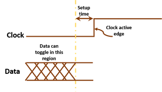
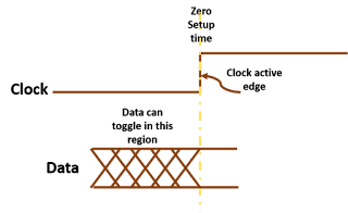
As we know from the definition of setup time, setup time is a point on time axis which restrains data from changing after it. Data can change only before occurrence of setup timing point. Theoretically, there is no constraint on occurrence of setup time point with respect to clock active edge. It can either be before, after or at the same time as that of clock edge. Depending upon the relative occurrence of setup time point and clock active edge, setup time is said to be positive, zero or negative.

Positive setup time: When setup time point is  before the arrival of clock edge, setup time is said to be positive. Figure 1 below shows positive setup time.
When setup time point is  before the arrival of clock edge, setup time is said to be positive.
Figure 1: Positive setup time


Zero setup time: When setup time point is at the same instant as clock's active edge, setup time is said to be zero. Figure 2 shows a situation wherein setup time is zero.

When setup time point is at the same instant as clock's active edge, setup time is said to be zero.
Figure 2: Zero setup time


Negative setup time: When setup time point occurs after clock edge, setup time is said to be negative. Figure 3 shows timing waveform for negative setup time.
When setup time point occurs after clock edge, setup time is said to be negative.
Figure 3: Negative setup time


What causes different values of setup time: We have discussed above theoretical aspects of positive, zero and negative setup time. Let us go a bit deeper into the details. Figure 4 shows a positive level-sensitive D-latch. As we know from the definition of setup time, setup time depends upon the relative arrival times of data and clock at input transmission gate (We have to ensure data has reached upto NodeD when clock reaches input transmission gate). Depending upon the relative arrival times of data and clock, setup time can be positive, zero or negative.
Figure 4: Positive level-sensitive latch
Let us assume the delay of an inverter is 1 ns. Then, to ensure that the data has reached NodeD when clock edge arrives at input transmission gate, data has to be available at the input transmission gate at least 2 ns before. So, if both data and clock reach the reference point at the same time, the latch has a setup time of 2 ns.

Now, if data takes 1 ns more than clock to reach input transmission gate from the reference point, then, data has to reach reference point at least 3 ns before clock reference point. In this case, setup time will be 3 ns.

Similarly, if data takes 1 ns less than clock to reach input transmission gate, setup time will be 1 ns. And if data takes 2 ns less than clock to reach input transmission gate, setup time will be zero.

Now, if there is further difference between delays of data and clock from respective reference points to input transmission gate, the hold time will become negative. For example, if data takes 3 ns less than clock to reach input transmission gate, setup time will be -1 ns.

This is how setup time depends upon relative delays of data and clock within the sequential element. And it completely makes sense to have negative setup time.

Also read:

Positive, negative and zero hold time


As we know from the definition of hold time, hold time is a point on time axis which restrains data from changing before it. Data can change only after hold time has elapsed. Now, there is no constraint on the occurrence of hold time point with respect to clock edge. It can either be after, before or at the same instant of time as that of clock active edge.

Posotive hold time: When hold time point is after the arrival of clock active edge, hold time is said to be positive hold time. Figure 1 below shows positive hold time.

Positive hold time, hold time, data can toggle after clock edge, data needs to be stable at least for hold time after clock edge
Figure 1: Positive hold time


Zero hold time: When hold time point is at the same time instant as that of clock active edge, we say that hold time of the sequential element is zero. Figure 2 below shows timing waveform for zero hold time.


Data can toggle right after clock edge
Figure 2: Zero hold time


Negative hold time: Similarly, when hold time point comes earlier on time scale as compared to data, we say that hold time of the sequential element is negative. Figure 3 shows timing waveform for negative hold time.

Negative hold time allows data to toggle even before clock ege
Figure 3: Negative hold time


We have discussed above theoretical aspects of positive, zero and negative hold time. Let us go a bit deeper into the details. Figure 4 shows a positive level-sensitive D-latch. As we know (from definition of hold time), hold time depends upon the relative arrival times of clock and data at the input transmission gate (We have to ensure data does not reach NodeC). Depending upon the times of arrival of clock and data, hold time can be positive or negative.

Figure 4: Positive level-sensitive D-latch

Let us say, the delay of an inverter is 1 ns. Then, we can afford the data to reach transmission gate input even 0.9 ns before arrival of clock at transmission gate. This will ensure data reaches NodeC (-0.9 + 1 =) 0.1 n after arrival of clock edge, if allowed. But, since, clock closes transmission gate, data will not reach NodeC. So, in this case, hold time is -1 ns. If the delay from NodeB to NodeC was something else, hold time would also have been different.

Now, if we say that clock arrives at transmission gate 1 ns earlier than data, then, by above logic, hold time of this latch will be -2 ns.

Similarly, if clock arrives at transmission gate 0.5 ns after data, hold time will be -0.5 ns.

And if clock arrive at transmission gate 1 ns after data, hold time will be  zero.

If the arrival time of clock is made more late, hold time will be greater than zero. For example, if arrival time of clock is 2 ns after data, hold time will be +1 ns.


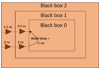
Hold time of the circuit is also dependent upon the reference point. For example, consider a multi-level black box as shown in figure 5. If we look at black box 0, its hold time is -1 ns. At level of black box 1, wherein clock travels 2 ns and data travels 0.5 ns to reach black box 0, hold time is (-1 + 2 - 0.5 = ) 0.5 ns. Similarly, at the level of black box 2, hold time is 1 ns. This is how, hold time depends upon the relative arrival times of clock and data. And it completely makes sense to have a negative hold time.

DFT basics

DFT stands for Design For Testification. DFT engineers try to make the testing of design more cost effective by introducing some structures into the design itself. By doing so, the overall test cost, and hence, cost of production comes down. Below, we list some of our posts covering the basics of DFT. Please provide your feedbacks regarding the topics you want to see as a part of this list. :-) Happy learning.

Setup time vs hold time

In digital designs, each and every sequential element has some restrictions related to the data with respect to clock in the form of windows in which data can change or not. There is always a region around the active edge of the clock in which data is not allowed to change at the input of the sequential element. This is because, if the data changes at the input within this window, we cannot guarantee the output. If this happens, there can be one of the three possibilities:
  • Current output data can be the result of current input data
  • Current output data can be the result of previous input data
  • The output can go metastable (as explained in metastability)
This region around clock edge is marked by two boundary lines, one perrtaining to setup time, and other to hold time. The region between these two lines is generally termed as setup-hold window. Figure 1 below shows the setup-hold window.
Figure 1: Figure showing setup/hold window of a sequential element
There are certain points of difference between setup time and hold time that we need to keep in mind:
  • Setup time signifies the point in time before which data needs to be stable, whereas hold time is the point of time after which the data needs to be stable
  • Adherence to setup time ensures that the data launched at previous active clock edge by another flip-flop gets captured at the current clock edge. On the other hand, adherence to hold time ensures that the data launched at the current edge does not get captured on the same edge.
  • Above point also means that setup time adherence ensures that the design goes to next state smoothly, whereas hold time adherence means the current state is not disturbed.
Hope this post helped you in understanding the basic difference in setup time and hold time.

Also read:

Propagation delay of a net

Definition of net propagation delay: The propagation delay of a net can be defined as the amount of time it takes a logic signal to propagate from the output of one logic gate to the input of another. Normally, it is defined as the difference between the times when the output of driver gate of net reaches 50% of its final value to when the input of the load cell of net reaches 50% of its final value.

How net delay is calculated: The net delay is calculated from the parasitics of the net. The parasitics are calculated based upon the topology of the net. These may also be read in from the parasitics file (SPEF, DSPF etc). The resulting RC-circuit resulting from the net topology is, then, simulated using certain algorithms (cosidering speed and accuracy requirements) for net delay.

Hold time

Definition of hold time: Hold time is defined as the minimum amount of time after arrival of clock's active edge so that it can be latched properly. In other words, each flip-flop (or any sequential element, in general) needs data to be stable for some time after arrival of clock edge such that it can reliably capture the data. This amount of time is known as hold time.

We can also link hold time with state transitions. We know that the data to be captured at the current clock edge was launched at previous clock edge by some other flip-flop. And the data launched at the current clock edge must be captured at the next edge. Adherence to hold time ensures that the data launched at current edge is not captured at the current clock edge. And the data launched at previous edge is captured and not disturbed by the one launched at current edge. In other words, hold time ensures that the current state of the design is not disturbed.

Figure 1 : Hold time


Figure 1 shows that data is allowed to toggle after the yellow dotted line. This yellow dotted line corresponds to hold time. The time difference between the active clock edge and this yellow dotted line is hold time. Data cannot toggle before this yellow dotted line for a duration known as setup-hold window. Occurrence of such an event is termed as hold violation. The consequence of such a violation can be capture of wrong data (better termed as hold check violation) or the sequential element going into meta-stable state (hold time violation).


Figure 2: A positive level-sensitive D-latch
Latch hold time: Figure 2 shows a positive level-sensitive latch. If there is a toggling of data at the latch input close to negative edge (while the latch is closing), there will be an uncertainty as if data will be capture reliably or not. For data to be captured reliably, next data must not reach Node C when closing edge of clock arrives at the input transmission gate. For this to happen, data must not travel NodeA -> NodeB -> NodeC before clock edge arrives. Data must change after this time interval only. 

Flip-flop hold time: Figure 3 below shows a master-slave negative edge-triggered D flip-flop using transmission gate latches. This is the most popular configuration of a flip-flop used in today's designs. Let us get into the details of hold time for this flip-flop. For this flip-flop to capture data reliably, new data must not be present at nodeD at the arrival of negative edge of clock. So, data must not travel NodeA -> NodeB -> NodeC -> NodeD when clock edge arrives. For data to not reach NodeD when clock edge arrives, it must toggle after some interval A with respect to clock. This interval corresponds to hold time of the flip-flop.We can also say that the hold time of flip-flop is, in a way, hold time of master latch.
 A D-type flip-flop consists of two latches connected back to back in master-slave format
Figure 3: D-flip flop

Hope this helped you in understanding the basics of hold time. You can suggest any improvement you think below in comments.

Setup and hold interview questions

Almost every interview for a VLSI design engineer has at least a question related to setup and hold. So, it is very important to prepare well. We list below a few topics related to setup and hold that may prove to be more than useful for setup and hold related interview questions.


Please share your interview experiences with us in comments so that these can be of help to other readers. Also, if you have any suggestion for us, you can get in touch with us. All the best. :-)

Liberty format : an introduction

What is liberty format: Liberty format is an industry standard format used to describe library cells of a particular technology. A cell could be a standard cell, IO Buffer, complex IP etc. Library cell description contains a lot of information like timing information, power estimation, other several attributes like area, functionality, operating condition etc. Speaking more technically, liberty format is a format to represent timing and power properties of black boxes (which we cant descend into). Liberty is an ASCII format, usually represented in a text file with extension ".lib". In this section, we will discuss timing aspects (delay and transition times) related to liberty format.

How is liberty file populated with data: The cells represented through liberty files are first simulated under a variety of conditions representative of actual design conditions that the cell may be exposed to. This process is known as characterization of library cells. As a very simple example, the delay of an inverter depends upon the input transition time and output load capacitance seen by it. The inverter will be characterized for a range of input transitions and output load capacitances. This characterization data, will then, be put into liberty in the form of a look-up table representing delay values at different transition times and load values.

To understand the different constructs related to timing in liberty file, let us take example of inverter. Rising transition at the input of inverter produces falling transition at the output of inverter and vice-versa. Hence there are two types of delay :

  1. Rise delay : It is the propagation delay (see definition) between output and input when output changes from 0 to 1.
  2. Output fall delay : It is the propagation delay between output and input when output is changing from 1 to 0.
In the real world, signal does not change its state from 0 to 1 or 1 to 0 abruptly. It takes some time to change its state. Hence, delay is measured based upon the threshold points. Threshold points in the liberty file are specified as below:


# threshold point of input falling edge
input_threshold_pct_fall : 50.0 ;

# threshold point of input rising edge
input_threshold_pct_rise : 50.0 ;

#threshold point of output falling edge
output_threshold_pct_fall : 50.0 ;

#threshold point of output rising edge
output_threshold_pct_rise : 50.0 ;


NOTE : these values are in percentage. e.g. If vdd is 5v then all of the above values will be 2.5.

So, Output rise delay is time difference between output_threshold_pct_rise and input_threshold_pct fall. Similarly Output fall delay is time difference between output_threshold_pct_fall and input_threshold_pct_rise.

Transition time : Time it takes for a signal to changes its state from one level to another level. Transition time is represented in terms of slew in liberty. Actually slew is inversely proportional to transition time. More the transition time, lesser is the slew rate and vice-versa. As we know that
voltage transition at the output is :
V = Vdd * [ 1 - e^ ( -t/(RC ) ) ] 

As Voltage equation is exponential, the voltage waveform is asymptotic at ends It is difficult to determine the exact start and end point of transition hence transition time is defined in terms of threshold values as follow :


# lower threshold point for falling  edge

slew_lower_threshold_pct_fall  : 30;

# upper threshold point for falling  edge
slew_upper_threshold_pct_fall : 30;

# lower threshold point for rising  edge
slew_lower_threshold_pct_rise : 70;

# upper threshold point for rising  edge
slew_upper_threshold_pct_rise : 70;

Reading from a file in tcl

It is very common to read from and/or write to a file in any programming language. In tcl also, one frequently uses file operations. read command in tcl reads the entire file and stores it into a variable. One can, then, perform the desired operations onto the read data. The normal command sequence to read a file in tcl language is as below:

// script to read and display contents
set infile [open input_file.rpt r] // Create a file pointer and point it to the file to be read
set file_data [read $infile]            // Assign file_data with contents of infile
close $infile                                        // Detach the file pointer from file to be read
set lines [split $file_data “\n”]   
// Split the file contents by lines and assign each line to an element of list
foreach element $lines {
                puts $element                  // Display each element of $lines onto screen.
}

2-input AND gate using 2:1 mux

2-input AND gate implementation using 2:1 mux: Figure 1 below shows the truth table of a 2-input AND gate. If we observe carefully, OUT equals '0' when A is '0'. And OUT follows B when A is '1'. So, if we connect A to the select pin of a 2:1 mux, AND gate will be implemented if we connect D0 to '0' and D1 to 'B'.

A 2-input AND gate has output '0' when either or both inputs is '0'. And output is '1' when both the inputs are '1'.
Figure 1: Truth table of AND gate
Figure 2 below shows the implementation of 2-input AND gate using a 2:1 multiplexer.

An AND gate can be implemented using a 2-input multiplexer by connected D0 input to '0' and D1 to B, SEL being connected to A. AND gate using mux, AND gate using 2x1 mux, 2-input AND gate using mux
Figure 2: Implementation of AND gate using a 2:1 mux

Also read:

2-input NAND gate using 2:1 mux

2-input NAND gate using 2:1 mux: Figure 3 below shows the truth table of a 2-input NAND gate. If we observe carefully, OUT equals '1' when A is '0'. Similarly, when A is '1', OUT is B'. So, if we connect SEL pin of mux to A, D0 pin of mux to '1' and D1 to B', then it will act as a NAND gate.

In a 2-input NAND gate, output is '0' when both inputs are '1', otherwise output is '1'
Figure 3: Truth table of 2-input NAND gate

Figure 4 below shows the implementation of a 2-input NAND gate using 2:1 mux.


A NAND gate can be implemented using a 2-input multiplexer, if we connect the select pin of the multiplexer to A, D0 to VDD and D1 to B' inputs. NAND gate using mux, NAND gate using 2x1 mux
Figure 4: Implementation of 2-input NAND gate using 2:1 mux

Also read:

2-input OR gate using 2:1 mux

2-input OR gate using 2x1 mux: Figure 5 below shows the truth table for a 2-input OR gate. If we observe carefully, OUT equals B when A is '0'. Similarly, OUT is '1' (or A), when A is '1'. So, we can make a 2:1 mux act like a 2-input OR gate, if we connect D0 pin to B and D1 pin to A, with select connected to A.

In a 2-input OR gate, output is '1' when either or both of the inputs are '1'. Otherwise, output is '0'.
Figure 5: Truth table of 2-input OR gate

Figure 6 below shows the implementation of 2-input OR gate using a 2:1 multilpexer:


A 2-inputs multiplexer can be converted to an OR gate, if we connect the select pin of mux to A-input, D0 to B-input and D1 to VDD. OR gate using mux, OR gate using 2x1 mux
Figure 6: Implementation of 2-input OR gate using 2:1 mux

Also read:

2-input XNOR gate using 2:1 mux

2-input XNOR gate using 2x1 mux: Figure 1 below shows the truth table of a 2-input XNOR gate. If we observe carefully, OUT equals B' when A is '0' and equals B when A is '1'. So, a 2-input XNOR gate can be implemented from a 2x1 mux, if we connect SEL pin to A, D0 to B' and D1 to B.

In a 2-input XNOR gate, output equals '0' when exactly one of the inputs is '1', otherwise output is '1'.
Figure 1: Truth table of 2-input XNOR gate
The implementation of 2-input XOR gate using a 2x1 mux is as shown in figure 2.
A 2-input XNOR gate can be realized using a 2:1 mux provided we connect the select to A-input, D0 to B' and D1 to B. XNOR gate using mux, XNOR gate using 2x1 mux, 2-input XNOR gate using mux
Figure 2: Implementation of 2-input XNOR gate using 2x1 mux

Similarly, we can observe the output for different values of B and follow the same steps to obtain the XNOR gate implementation.