Setup time vs hold time

In digital designs, each and every sequential element has some restrictions related to the data with respect to clock in the form of windows in which data can change or not. There is always a region around the active edge of the clock in which data is not allowed to change at the input of the sequential element. This is because, if the data changes at the input within this window, we cannot guarantee the output. If this happens, there can be one of the three possibilities:
  • Current output data can be the result of current input data
  • Current output data can be the result of previous input data
  • The output can go metastable (as explained in metastability)
This region around clock edge is marked by two boundary lines, one perrtaining to setup time, and other to hold time. The region between these two lines is generally termed as setup-hold window. Figure 1 below shows the setup-hold window.
Figure 1: Figure showing setup/hold window of a sequential element
There are certain points of difference between setup time and hold time that we need to keep in mind:
  • Setup time signifies the point in time before which data needs to be stable, whereas hold time is the point of time after which the data needs to be stable
  • Adherence to setup time ensures that the data launched at previous active clock edge by another flip-flop gets captured at the current clock edge. On the other hand, adherence to hold time ensures that the data launched at the current edge does not get captured on the same edge.
  • Above point also means that setup time adherence ensures that the design goes to next state smoothly, whereas hold time adherence means the current state is not disturbed.
Hope this post helped you in understanding the basic difference in setup time and hold time.

Also read:

Propagation delay of a net

Definition of net propagation delay: The propagation delay of a net can be defined as the amount of time it takes a logic signal to propagate from the output of one logic gate to the input of another. Normally, it is defined as the difference between the times when the output of driver gate of net reaches 50% of its final value to when the input of the load cell of net reaches 50% of its final value.

How net delay is calculated: The net delay is calculated from the parasitics of the net. The parasitics are calculated based upon the topology of the net. These may also be read in from the parasitics file (SPEF, DSPF etc). The resulting RC-circuit resulting from the net topology is, then, simulated using certain algorithms (cosidering speed and accuracy requirements) for net delay.

Hold time

Definition of hold time: Hold time is defined as the minimum amount of time after arrival of clock's active edge so that it can be latched properly. In other words, each flip-flop (or any sequential element, in general) needs data to be stable for some time after arrival of clock edge such that it can reliably capture the data. This amount of time is known as hold time.

We can also link hold time with state transitions. We know that the data to be captured at the current clock edge was launched at previous clock edge by some other flip-flop. And the data launched at the current clock edge must be captured at the next edge. Adherence to hold time ensures that the data launched at current edge is not captured at the current clock edge. And the data launched at previous edge is captured and not disturbed by the one launched at current edge. In other words, hold time ensures that the current state of the design is not disturbed.

Figure 1 : Hold time


Figure 1 shows that data is allowed to toggle after the yellow dotted line. This yellow dotted line corresponds to hold time. The time difference between the active clock edge and this yellow dotted line is hold time. Data cannot toggle before this yellow dotted line for a duration known as setup-hold window. Occurrence of such an event is termed as hold violation. The consequence of such a violation can be capture of wrong data (better termed as hold check violation) or the sequential element going into meta-stable state (hold time violation).


Figure 2: A positive level-sensitive D-latch
Latch hold time: Figure 2 shows a positive level-sensitive latch. If there is a toggling of data at the latch input close to negative edge (while the latch is closing), there will be an uncertainty as if data will be capture reliably or not. For data to be captured reliably, next data must not reach Node C when closing edge of clock arrives at the input transmission gate. For this to happen, data must not travel NodeA -> NodeB -> NodeC before clock edge arrives. Data must change after this time interval only. 

Flip-flop hold time: Figure 3 below shows a master-slave negative edge-triggered D flip-flop using transmission gate latches. This is the most popular configuration of a flip-flop used in today's designs. Let us get into the details of hold time for this flip-flop. For this flip-flop to capture data reliably, new data must not be present at nodeD at the arrival of negative edge of clock. So, data must not travel NodeA -> NodeB -> NodeC -> NodeD when clock edge arrives. For data to not reach NodeD when clock edge arrives, it must toggle after some interval A with respect to clock. This interval corresponds to hold time of the flip-flop.We can also say that the hold time of flip-flop is, in a way, hold time of master latch.
 A D-type flip-flop consists of two latches connected back to back in master-slave format
Figure 3: D-flip flop

Hope this helped you in understanding the basics of hold time. You can suggest any improvement you think below in comments.

Liberty format : an introduction

What is liberty format: Liberty format is an industry standard format used to describe library cells of a particular technology. A cell could be a standard cell, IO Buffer, complex IP etc. Library cell description contains a lot of information like timing information, power estimation, other several attributes like area, functionality, operating condition etc. Speaking more technically, liberty format is a format to represent timing and power properties of black boxes (which we cant descend into). Liberty is an ASCII format, usually represented in a text file with extension ".lib". In this section, we will discuss timing aspects (delay and transition times) related to liberty format.

How is liberty file populated with data: The cells represented through liberty files are first simulated under a variety of conditions representative of actual design conditions that the cell may be exposed to. This process is known as characterization of library cells. As a very simple example, the delay of an inverter depends upon the input transition time and output load capacitance seen by it. The inverter will be characterized for a range of input transitions and output load capacitances. This characterization data, will then, be put into liberty in the form of a look-up table representing delay values at different transition times and load values.

To understand the different constructs related to timing in liberty file, let us take example of inverter. Rising transition at the input of inverter produces falling transition at the output of inverter and vice-versa. Hence there are two types of delay :

  1. Rise delay : It is the propagation delay (see definition) between output and input when output changes from 0 to 1.
  2. Output fall delay : It is the propagation delay between output and input when output is changing from 1 to 0.
In the real world, signal does not change its state from 0 to 1 or 1 to 0 abruptly. It takes some time to change its state. Hence, delay is measured based upon the threshold points. Threshold points in the liberty file are specified as below:


# threshold point of input falling edge
input_threshold_pct_fall : 50.0 ;

# threshold point of input rising edge
input_threshold_pct_rise : 50.0 ;

#threshold point of output falling edge
output_threshold_pct_fall : 50.0 ;

#threshold point of output rising edge
output_threshold_pct_rise : 50.0 ;


NOTE : these values are in percentage. e.g. If vdd is 5v then all of the above values will be 2.5.

So, Output rise delay is time difference between output_threshold_pct_rise and input_threshold_pct fall. Similarly Output fall delay is time difference between output_threshold_pct_fall and input_threshold_pct_rise.

Transition time : Time it takes for a signal to changes its state from one level to another level. Transition time is represented in terms of slew in liberty. Actually slew is inversely proportional to transition time. More the transition time, lesser is the slew rate and vice-versa. As we know that
voltage transition at the output is :
V = Vdd * [ 1 - e^ ( -t/(RC ) ) ] 

As Voltage equation is exponential, the voltage waveform is asymptotic at ends It is difficult to determine the exact start and end point of transition hence transition time is defined in terms of threshold values as follow :


# lower threshold point for falling  edge

slew_lower_threshold_pct_fall  : 30;

# upper threshold point for falling  edge
slew_upper_threshold_pct_fall : 30;

# lower threshold point for rising  edge
slew_lower_threshold_pct_rise : 70;

# upper threshold point for rising  edge
slew_upper_threshold_pct_rise : 70;

Reading from a file in tcl

It is very common to read from and/or write to a file in any programming language. In tcl also, one frequently uses file operations. read command in tcl reads the entire file and stores it into a variable. One can, then, perform the desired operations onto the read data. The normal command sequence to read a file in tcl language is as below:

// script to read and display contents
set infile [open input_file.rpt r] // Create a file pointer and point it to the file to be read
set file_data [read $infile]            // Assign file_data with contents of infile
close $infile                                        // Detach the file pointer from file to be read
set lines [split $file_data “\n”]   
// Split the file contents by lines and assign each line to an element of list
foreach element $lines {
                puts $element                  // Display each element of $lines onto screen.
}

2-input AND gate using 2:1 mux

2-input AND gate implementation using 2:1 mux: Figure 1 below shows the truth table of a 2-input AND gate. If we observe carefully, OUT equals '0' when A is '0'. And OUT follows B when A is '1'. So, if we connect A to the select pin of a 2:1 mux, AND gate will be implemented if we connect D0 to '0' and D1 to 'B'.

A 2-input AND gate has output '0' when either or both inputs is '0'. And output is '1' when both the inputs are '1'.
Figure 1: Truth table of AND gate
Figure 2 below shows the implementation of 2-input AND gate using a 2:1 multiplexer.

An AND gate can be implemented using a 2-input multiplexer by connected D0 input to '0' and D1 to B, SEL being connected to A. AND gate using mux, AND gate using 2x1 mux, 2-input AND gate using mux
Figure 2: Implementation of AND gate using a 2:1 mux

Also read:

2-input NAND gate using 2:1 mux

2-input NAND gate using 2:1 mux: Figure 3 below shows the truth table of a 2-input NAND gate. If we observe carefully, OUT equals '1' when A is '0'. Similarly, when A is '1', OUT is B'. So, if we connect SEL pin of mux to A, D0 pin of mux to '1' and D1 to B', then it will act as a NAND gate.

In a 2-input NAND gate, output is '0' when both inputs are '1', otherwise output is '1'
Figure 3: Truth table of 2-input NAND gate

Figure 4 below shows the implementation of a 2-input NAND gate using 2:1 mux.


A NAND gate can be implemented using a 2-input multiplexer, if we connect the select pin of the multiplexer to A, D0 to VDD and D1 to B' inputs. NAND gate using mux, NAND gate using 2x1 mux
Figure 4: Implementation of 2-input NAND gate using 2:1 mux

Also read:

2-input OR gate using 2:1 mux

2-input OR gate using 2x1 mux: Figure 5 below shows the truth table for a 2-input OR gate. If we observe carefully, OUT equals B when A is '0'. Similarly, OUT is '1' (or A), when A is '1'. So, we can make a 2:1 mux act like a 2-input OR gate, if we connect D0 pin to B and D1 pin to A, with select connected to A.

In a 2-input OR gate, output is '1' when either or both of the inputs are '1'. Otherwise, output is '0'.
Figure 5: Truth table of 2-input OR gate

Figure 6 below shows the implementation of 2-input OR gate using a 2:1 multilpexer:


A 2-inputs multiplexer can be converted to an OR gate, if we connect the select pin of mux to A-input, D0 to B-input and D1 to VDD. OR gate using mux, OR gate using 2x1 mux
Figure 6: Implementation of 2-input OR gate using 2:1 mux

Also read:

2-input XNOR gate using 2:1 mux

2-input XNOR gate using 2x1 mux: Figure 1 below shows the truth table of a 2-input XNOR gate. If we observe carefully, OUT equals B' when A is '0' and equals B when A is '1'. So, a 2-input XNOR gate can be implemented from a 2x1 mux, if we connect SEL pin to A, D0 to B' and D1 to B.

In a 2-input XNOR gate, output equals '0' when exactly one of the inputs is '1', otherwise output is '1'.
Figure 1: Truth table of 2-input XNOR gate
The implementation of 2-input XOR gate using a 2x1 mux is as shown in figure 2.
A 2-input XNOR gate can be realized using a 2:1 mux provided we connect the select to A-input, D0 to B' and D1 to B. XNOR gate using mux, XNOR gate using 2x1 mux, 2-input XNOR gate using mux
Figure 2: Implementation of 2-input XNOR gate using 2x1 mux

Similarly, we can observe the output for different values of B and follow the same steps to obtain the XNOR gate implementation.

8x1 multiplexer using 4x1 multiplexer

An 8x1 mux can be implemented using two 4x1 muxes and one 2x1 mux. 4 of the inputs can first be decoded using each 4-input mux using two least significant select lines (S0 and S1). The output of the two 4x1 muxes can be further multiplexed with the help of MSB of select lines at further stage. The implementation of 8x1 using 4x1 and 2x1 muxes is shown in figure 1 below:


2-input NOR gate using 2:1 mux

2-input NOR gate using 2x1 mux: Figure 1 below shows the truth table of a 2-input NOR gate. If we observe carefully, OUT equal B' when A is '0'. Similarly, OUT equals '0' when A is '1'. So, we can make a 2-input mux act like a 2-input NOR gate, if we connect SEL of mux to A, D0 to B' and D1 to '0'.

In a 2-input NOR gate, output equals '0' when either or both the inputs is '1'. Otherwise, output is '0'.
Figure 1: Truth table of 2-input NOR gate
Figure 2 shows the implementation of 2-input NOR gate using 2:1 mux.


NOR gate using mux, 2-input NOR gate using 2:1 mux, NOR gate using 2x1 mux
Figure 2: Implementation of 2-input NOR gate using 2x1 mux

Similarly, we can connect B to select pin of mux and follow the same procedure of observation from truth table to get the NOR gate implemented.

Also read:

Matchstick game bonanza!!

Problem: There are 'N' matchsticks placed on the table. You and your opponent are to pick any number of matchsticks between 1 and 5. Its your turn first. The one picking the last stick loses the game. You have to device a strategy such that you always win the game.Also, is there any starting number that cannot guarantee that you always win?

Solution: Here, you have to ensure that the control of the game always remains in your hands. Let us approach this problem from the last. The last matchstick has to be picked by your opponent so as to ensure your win. So, your last turn must ensure that there must be only one matchstick left on the table. If this is not the case, say there are 2 matchsticks. Then, your opponent will pick 1 stick and you are left with only one stick to pick and lose the game.
Similarly, one turn before last of your opponent, there must be more than 6 sticks so that he cannot leave you with 1 stick by picking 5 of them. But if there are more than 7 sticks, he may leave you with the same situation by leaving 7 on the table. If you leave 7, the other can at max pick 5 and min 1 leaving any number between 6 and 2 on the table. You can now pick the desired number leaving the last stick to be picked by him. Now, if there were 8 sticks on the table, your opponent would pick 1 leaving you with 7 sticks. :-( Similarly, one turn before, you should have left 13 sticks on the table.

So, your approach should be to leave (6M + 1) sticks on the table always. Ensure that at the end of each round, 6 less matchsticks are there on the table. (For instance, if your opponent picks 3 sticks, you also pick 3).

But there is a catch in this game, if there are already (6M + 1) sticks on the table initially, and its your turn first, you cannot ensure after your first turn the winning strategy. Now, the control goes into the hand of your opponent and you are at the verge of losing the game.

Similarly, 5 can be replaced with any number 'K'. At the end of each turn, you have to ensure there are (K+1)M + 1 sticks left on the table.

2-input XOR gate using 2:1 mux

2-input XOR gate using 2x1 mux: Figure 1 shows the truth table for a 2-input XOR gate where A and B are the two inputs and OUT is equal to XOR of A and B. If we observe carefully, OUT equals B when A is '0' and B' when A is '1'. So, a 2:1 mux can be used to implement 2-input XOR gate if we connect SEL to A, D0 to B and D1 to B'.

In a 2-input XNOR gate, output equals '1' when exactly one of the inputs is '1', otherwise output is '0'.
Figure 1: Truth table of 2-input XOR gate
Figure 2 shows the implementation of 2-input XOR gate using 2x1 mux.

A 2-input XNOR gate can be realized using a 2:1 mux provided we connect the select to A-input, D0 to B and D1 to B'. XOR gate using mux, 2-input XNOR gate using mux, XNOR gate using 2:1 mux
Figure 2: Implementation of 2-input XOR gate using 2x1 mux

Similarly, we can connect B to select of mux, and get the XOR gate implemented using similar procedure.

NOT gate using 2:1 mux


NOT gate using 2:1 mux: Figure 13 shows the truth table for a NOT gate. The only inverting path in a multiplexer is from select to output. To implement NOT gate with the help of a mux, we just need to enable this inverting path. This will happen if we connect D0 to '1' and D1 to '0'.

Truth table of NOT gate

Figure 1: Truth table of NOT gate

We can also say that we need to propagate '0' to output when input (select) is 1 and '1' when input is '0'. Figure 14 shows the implementation of NOT gate using 2x1 mux:


A not gate can be implemented by connecting input to the select line of mux. '1' can be connected to D0 and '0' can be connected to D1.
Figure 2: NOT gate implementation using 2:1 mux

Also read:

Zero cycle paths

Zero cycle path: A zero cycle timing path is a representative of race condition between data and clock. A zero cycle path is one in which data is launched and captured on the same edge of the clock. In other words, setup check for a zero cycle path is zero cycle, i.e., it is on the same edge as the one launching data. Hold check, then, will be one cycle before the edge at which data is launched. Figure 1 below shows the setup check and hold check for a zero cycle timing path.


In a zero cycle path, setup check is zero cycle. In other words, it is on the same edge as of launch clock.
Figure 1: Setup check and hold check for zero cycle paths


How to specify zero cycle path: As we know, by default, setup check is single cycle (is checked on the next edge with respect to the one on which data is launched). If the FSM requires a timing path to be zero cycle, it has to be specified using the SDC command "set_multicycle_path".

Default setup check for a timing path is single cycle, whereas hold check is zero cycle.
Figure 2: Default setup and hold checks for single cycle timing path
The default setup and hold check for same edge timing paths is single cycle and zero cycle as shown in figure 2 above. To model it as a zero cycle path (as in figure 1), we need to apply following timing constraint:
set_multicycle_path 0 -setup -from <startpoint> -to <endpoint>
where <startpoint> is the the flip-flop which launches the data and <endpoint> is the flip-flop which captures the data. In other words, as viewed from application perspective, zero cycle path is one of the special cases of a multi-cycle path only. Above multicycle constraint modifies the setup check to be zero cycle. Hold check also, shifts one edge back.

Also read:

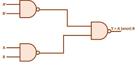
XNOR gate using NAND

As we know, the logical equation of a 2-input XNOR gate is given as below:
                      Y = A (xnor) B = (A' B '   +    A B)
Let us take an approach where we consider and A' as different variables for now (optimizations related to this, if any, will consider later). Thus, the logic equation, now, becomes:
                       Y = (CD    +    A B)           -----   (i)
     where
                      C = A'     and      D = B'
De-Morgan's law states that
                                m + n = (m'n')'

Taking this into account,
                     Y = ((CD)'(AB)')' = ((A' B')'  (A B)')'
Thus, Y is equal to ((A' nand B') nand (A nand B)). No further optimizations to the logic seem possible to this logic. Figure 1 below shows the implementation of XOR gate using 2-input NAND gates.
A 2 -input XOR gate implementation using NAND, XOR gate using NAND
Figure 1: 2-input XNOR gate implementation using NAND gates

2x1 mux using NAND gates

As we know, the logical equation of a 2-input mux is given as below:
                      Y = (s' A   +    s B)
Where s is the select of the multiplexer.
De-Morgan's law states that
                                m + n = (m'n')'

Taking this into account, here m = s'A  and  n = sB
                     Y = ((s'A)'(sB)')' = ((s' A)'  (s B)')'
Thus, Y is equal to ((s' nand A) nand (s nand B)). No further optimizations seem possible to this logic. Figure 1 below shows the implementation of 2:1 mux using 2-input NAND gates.
Figure 1: 2:1 Mux using NAND gates

3-input AND gate using 4:1 mux

As we know, a AND gate's output goes '1' when all its inputs are '1', otherwise it is '0'. The truth table for a 3-input AND gate is shown below in figure 1, where A, B and C are the three inputs and O is the output.
                                      O = A (and) B (and) C
Truth table for 3-input AND gate


A 4:1 mux has 2 select lines. We can connect A and B to each of the select lines. The output will, then, be a function of the third input C. Now, if we sub-partition the truth table for distinct values of A and B, we observe
When A = 0 and B = 0, O = 0 => Connect D0 pin of mux to '0'
When A = 0 and B = 1, O = 0 => Connect D1 pin of mux to '0'
When A = 1 and B = 0, O = 0 => Connect D2 pin of mux to '0'
When A = 1 and B = 1, O = C => Connect D3 pin of mux to C
The implementation of 3-input AND gate, based upon our discussion so far, is as shown in figure 2 below:


Also read:

3-input XOR gate using 2-input XOR gates


A 3-input XOR gate can be implemented using 2-input XOR gates by cascading 2 2-input XOR gates. Two of the three inputs will feed one of the 2-input XOR gates. The output of the first gate will, then, be XORed with the third input to get the final output.

Let us say, we want to XOR three inputs A,B and C to get the output Z. First, XOR A and B together to obtain intermediate output Y. Then XOR Y and C to obtain Z. The schematic representation to obtain 3-input XOR gate by cascading 2-input XOR gates is shown in figure below:

Implementation of 3-input XOR gate using 2-input XOR gates


Clock gating interview questions

One of the most important and frequently asked topics in interviews is clock gating and clock gating checks. We have a collection of blog-posts related to this topic which can help you master clock gating. You can go through following links to add to your existing knowledge of clock gating:

  • Clock gating checksDiscusses different clock gating structures used and associated timing checks related to these
  • Clock gating checks at a muxDiscusses clock gating checks that should be applied in case one of the inputs of mux has a clock signal connected to it, which is the most common clock gating check in today's designs


Our purpose is to make this page a single destination for any questions related to clock gating. If you have any source of related and additional information, please comment or send an email to myblogvlsiuniverse@gmail.com and we will add it here. Also, feel free to ask any question related to clock gating.

Puzzles and brainteasers

A lot of questions in interviews are related to puzzles and brainteasers and are meant to relate to the thought process of the candidate. Listing below a few of the puzzles that may be of interest to you.

Please feel free to share puzzles that you think may be of interest to others. 

Why NAND structures are preferred over NOR ones?

Both NAND and NOR are classified as universal gates, but we see that NAND is preferred over NOR in CMOS logic structures. Let us discuss why it is so:


We know that when output is at logic 1, pull up structure for the output stage is on and it provides a path from VDD to output. Similarly, pull down structure provides a path from GND to output when output is logic 0. Pull up and pull down resistances are one of major factor in determining the speed of cell. The inverse of pull up and pull down resistances are called output high drive and output low drive of the cell respectively. In general, cells are designed to have similar drive strength of pull up and pull down structures to have comparable rise and fall time.


NMOS has half the resistance of an equal sized PMOS. let us say resistance of a given sized NMOS is R then resistance of  PMOS of same size will be 2R. In NAND gate, two NMOS are connected in series and two PMOS are connected in parallel. So, pull up and pull down resistances will be:

            Pull up resistance = 2R || 2R = R
            Pull down resistance = R + R = 2R


On the other hand, in a NOR gate, two NMOS are connected in parallel and two PMOS are connected in series. The pull-up and pull-down resistances, now, will be:

            Pull up resistance = 2R + 2R = 4R
            Pull down resistance = R || R = R/2


NAND gate has better ratio of output high drive and output low drive as compared to NOR gate. Hence NAND gate is preferred over NOR.


To use NOR gate as universal gate either pull up or pull down structure has to be resized(decrease the length of PMOS cells or increase length of NMOS cells) to have similar resistance as resistance is directly proportional to length (length of channel here).

Also read:

Divide by 2 clock in VHDL

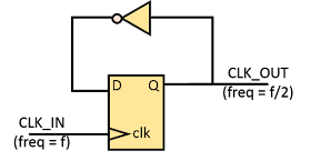
Clock dividers are ubiquitous circuits used in every digital design. A divide-by-N divider produces a clock that is N times lesser frequency as compared to input clock. A flip-flop with its inverted output fed back to its input serves as a divide-by-2 circuit. Figure 1 shows the schematic representation for the same.

A divide by 2 clock circuit produces output clock that is half the frequency of the input clock
Divide by 2 clock circuit
                                          
Following is the code for a divide-by-2 circuit.
-- This module is for a basic divide by 2 in VHDL.
library ieee;
use ieee.std_logic_1164.all;
entity div2 is
                port (
                                reset : in std_logic;
                                clk_in : in std_logic;
                                clk_out : out std_logic
                );
end div2;

-- Architecture definition for divide by 2 circuit
architecture behavior of div2 is
signal clk_state : std_logic;
begin
                process (clk_in,reset)
                begin
                                if reset = '1' then
                                                clk_state <= '0';
                                elsif clk_in'event and clk_in = '1' then
                                                clk_state <= not clk_state;
                                end if;
                end process;
clk_out <= clk_state;

end architecture;

Hope you’ve found this post useful. Let us know what you think in the comments.

Applications of latches


A latch is a level-sensitive storage element capable of storing 1-bit digital data (Read more about basics of latches here). However simple that may sound, but there are countless applications in digital VLSI circuits as discussed below:
  • Master-slave flip-flop: Cascading of a positive latch and negative latch gives a negative edge-triggered flip-flop and cascading of negative and positve latch gives a positive edge-triggered flip-flop. This kind of design of edge-triggered flip-flops is the most prevalent architecture used in VLSI industry. In other words, all the flip-flops used in today's designs are actually two latches cascaded back-to-back.
Figure 1: Master-slave flip-flops using latches

  • Latch as lockup element: A latch is used as a savior for scan hold timing closure in the form of lockup latch. A lockup latch is nothing more than a transparent latch used in places where hold timing is an issue due to either very large clock skew or uncommon path, one of the commonoly occuring scenarios being scan connection between two functionally non-interacting domains. Read more about lockup latch
  • Latches used for permormance gain: Latches, due to their inherent property of time borrowing, can capture data over a period of time, rather than at a particular instant. This property of latch can be taken advantage of by the stage having maximum delay borrowing time from next stage; thus, reducing overall clock period. Read more here
  • Latch pipeline: Going one step further, there can be a whole design implemented with latches. The basic principle used is that a positive latch must be succeeded by a negative latch, and vice-versa. Using a latch based design, we can effectively get the job done at half the clock frequency. But, it is not feasible to fulfil the requirement of positive latch output going to negative latch. The effort required to build even a small latch based pipeline (even as small as that shown below in figure 2) is very latge. That is why, we never see practically latch pipeline based circuits.
Figure 2: Latch pipeline

  • Integrated Clock Gating Cell: Latch is used in the path of enable signal in case of clock gating elements in order to avoid glitches. An AND gate, in general, requires enable to launch from negative edge-triggered flip-flop and vice-versa. But it is very difficult to generalize a state-machine. Hence, latches are embedded alongside the AND gate (or OR gate) as a single standard cell to be used at places where clock gating is required. Read more here.
  • Latches in memory arrays to store data: Regenerative latches are used inside memory arrays of SRAM to store data. Regenerative latch, in general, forms part of a memory bit-cell. The number of such bit cells is equal to the number of bits that the memory can store.
So, we have gone through a few of the applications of latches. Can you think of any other application of latches in designs? Please do not hesitate to share your knowledge with others. :-)