Default Setup/hold checks - positive flop to negative flop timing paths

The launch/capture event of a positive edge-triggered flip-flop happens on every positive edge of the clock, whereas that of a negative edge-triggered flip-flop occurs on the negative edge of the flip-flop. In this post, we will discuss the default setup/hold checks different cases - same clock, 1:n clock ratio clock and n:1 ratio clock. And this should cover all the possible cases of setup/hold checks.

Case 1: Both flip-flops getting same clock

Figure 1: Pos-flop to neg-flop default setup/hold checks when clocks are equal in frequency

Figure 1 shows a timing path from a positive edge-triggered flip-flop to a negative edge-triggered flip-flop. Let us say the data is launched at instant of time "T", which is a positive edge. Then, the next negative edge following time "T" serves as the edge which captures this data; thus forming the default setup check. And the very previous negative edge serves as the hold check. This is shown in the first part of figure 1. Thus, in this case, both setup and hold checks are half cycle.

Setup and hold slack equations

Setup slack = Period(clk)/2 + Tskew - Tclk_q - Tcomb - Tsetup

Hold slack = Period(clk)/2 + Tclk_q + Tcomb - Tskew - Thold


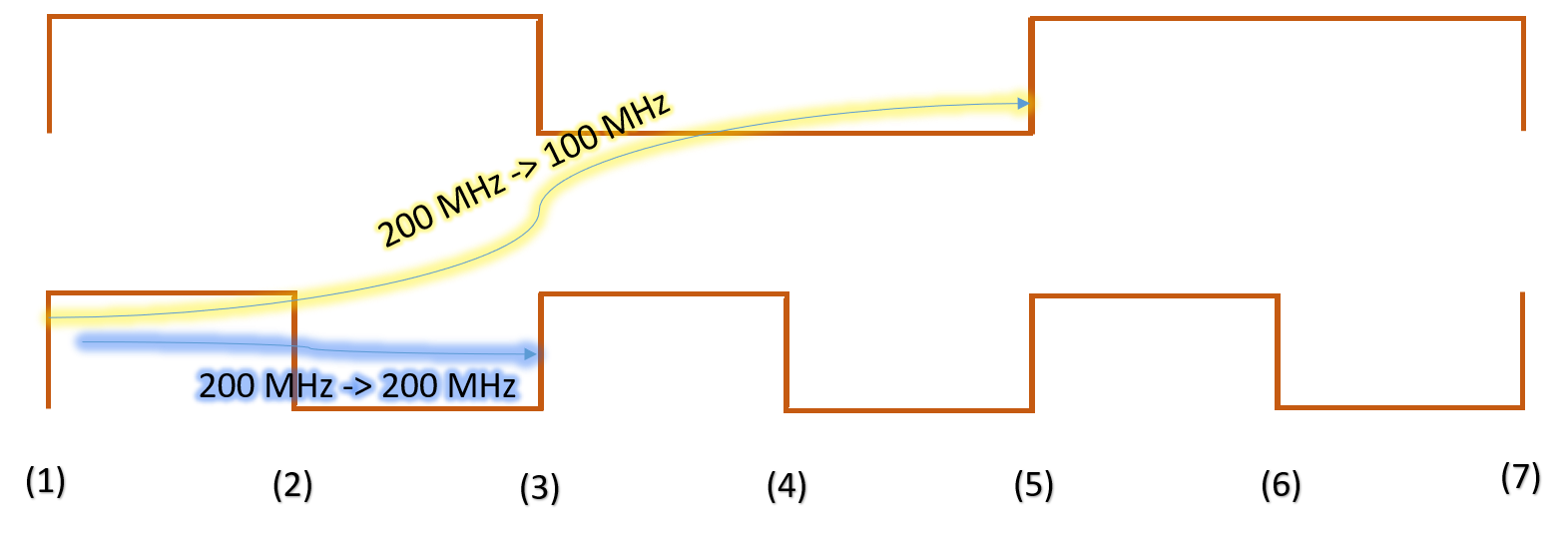
Case 2: Flip-flops getting clocks with frequency ratio N:1 and positive edge of launch clock coincides with negative edge of capture clock

One of the cases where this happens is when clock is divided by an even number. Another is when odd division is followed by inversion. The resulting waveform will be as shown in figure 2. In this case, each positive edge of launch flip-flop is capable of launching a fresh data, but will be overwritten by next data. Only the one which is launched on the positive edge closest to the negative edge of capture clock will get captured at the endpoint. Similarly, the data which is launched at the edge coinciding negative edge of capture clock must not overwrite the data captured at the same edge. The setup and hold checks, thus formed, are as shown in figure 2 below. The setup check is full cycle of launch clock, whereas hold check is a zero cycle check.


Figure 2: Default setup/hold checks for case 2

Setup and hold slack equations

Setup slack = period(launch_clock) + Tskew - Tclk_q - Tcomb - Tsetup

 Hold slack = Tclk_q + Tcomb - Tskew - Thold


Case 3: Flip-flops gettings clocks with frequency ration N:1 and positive edge of launch clock coincides with positive edge of capture clock

One of the cases where this happens is when capture of the data happens on an odd divided clock. The resulting setup and hold checks are as shown in figure 3. Both setup and hold checks are half cycle of faster launch clock.

Figure 3: Default setup/hold checks for case 3
Setup and hold slack equations

Setup slack = period(launch_clock)/2 + Tskew - Tclk_q - Tcomb - Tsetup

 Hold slack =  period(launch_clock)/2 + Tclk_q + Tcomb - Tskew - Thold

Case 4: Flip-flops getting clocks with frequency 1:N and positive edge of launch clock coincides with negative edge of capture clock

One of the cases is when division is performed after inversion of the master clock and data is launched on the divided clock. Figure 4 shows the default setup/hold checks for this case. In this case, setup check is equal to full cycle of faster clock and hold check is a zero cycle check.

Figure 4: Default setup/hold checks for case 4
Setup and hold slack equations

Setup slack = period(capture_clock) + Tskew - Tclk_q - Tcomb - Tsetup

 Hold slack = Tclk_q + Tcomb - Tskew - Thold

Case 5: Flip-flops getting clocks with frequency 1:N and positve edge of launch clock coincides with positive edge of capture clock

This is a case of even division, or inversion, followed by odd division, followed by inversion. The setup and hold checks, both are equal to half cycle of faster clock.

Setup and hold slack equations

Setup slack = period(capture_clock)/2 + Tskew - Tclk_q - Tcomb - Tsetup

 Hold slack =  period(capture_clock)/2 + Tclk_q + Tcomb - Tskew - Thold

Can you think of any other scenario of setup/hold checks for this case? Please feel free to share your views.


Clock relationship between reset synchronizer and fanout flip-flops

As we know, all flip-flops which are required to be "out of reset" at the same time are placed in fanout of a single reset synchronizer. In this post, we will discuss if there is any relationship required between clock frequency of reset synchronizer and the clock frequency of the flip-flops in fanout. For now, let us assume that all the flip-flops in the fanout of reset synchronizer work on a single clock "CLK". <dsfdsf> discussed the case when the flip-flops are working on multiple clocks.

Let us first assume that reset synchronizer's clock period is N*CLK_PERIOD; i.e. reset synchronizer gets a DIVIDE_BY_N clock of the flip-flops' clock. Figure 1 below shows the setup check from a clock with period N*CLK_PERIOD to a clock with period CLK_PERIOD. Since, all the flip-flops have same setup check being formed, all will get out of reset at the same edge; thus, fulfilling the requirement.


Similarly, there is a definite setup check from a clock with period CLK_PERIOD/N to a clock with period CLK_PERIOD as shown in figure 2 below. Thus, if reset synchronizer works on clock with frequency "N" times the flip-flops in fanout, we get all the flip-flops out of reset at same time, thereby, fulfilling the requirement again.


Thus, we see that if all the flip-flops in fanout of reset synchronizer work on a single clock, there is no relationship required between frequency of reset synchronizer and frequency of fanout flip-flops as long as we meet the setup and hold requierements.   However, this is not true when flip-flops work on multiple clocks as discussed in <SDFDSF>.


Design problem: Reset synchronizer clock for multi-frequency flip-flops in fanout

Design problem: A set of flip-flops, some working on 100 MHz clock and others working on 200 MHz clock are required to come out of reset together. What should be the clock of reset synchronizer

Solution: Since all the flip-flops are required to come out of reset in the same cycle, all these must get reset from a single reset synchronizer. Now, as the question states that the flip-flops in the fanout of reset synchronizer are working on two clocks. We need to find the correct-by-design clock that reset synchronizer should be working on. Let us assume that the correct clock to be connected to reset synchronizer is one of the two frequencies given.

Figure 1: Reset synchronizer


First, let us check by assuming that reset synchronizer works on positive edge of 100 MHz clock. Figure 2 shows the setup checks for 100 MHz -> 100 MHz and 100 MHz -> 200 MHz paths. Let us say, reset deassertion propagates to R1/Q at edge (1). Going by figure 2, all flip-flops working on 200 MHz clock will be out of reset at edge (3) and all flop-flops working on 100 MHz will be out of reset at edge (5). Thus, reset synchronizer working on positive edge of 100 MHz clock does not solve our purpose.

Figure 2: Reset synchronizer works on positive edge of 100 MHz clock


Now, let us check the same when reset synchronizer works on positive edge of 200 MHz clock. In this case, reset can deassert either on edge (1) or edge (3). If reset deasserts on edge 3, then, we have both the categories of flops coming out of reset at same time edge (5). But if reset deasserts on edge (1), both categories of flops get out of reset at different times. Thus, we can get the reset synchronizer working on 200 MHz clock, but we have to ensure by design that reset gets deasserted on the edge of 200 MHz clock that coincides with negative edge of 100 MHz clock. Figure 3 and figure 4 discuss these scenarios.

Figure 3: Reset synchronizer works on positive edge of 200 MHz clock coinciding with positive edge of 100 MHz clock


Figure 4: Reset synchronizer works on positive edge of 200 MHz clock coinciding with negative edge of 100 MHz clock

Same scenarios are expected as figure 3 & 4 when we make reset synchronizer work on negative edge of 200 MHz clock.

Now, let us explore the last option; i.e., reset synchronizer working on negative edge of 100 MHz clock. In this case, as shown in figure 5, both 100 MHz and 200 MHz flip-flops come out of reset on same edge. Thus, this case works perfectly. Figure 5 illustrates this.

Figure 5: Reset synchronizer works on negative edge of 100 MHz clock


Can you provide any other solution that is possible and better than ones discussed here.

Data check timing paths

Data check is a timing check, either picked from timing model or user-defined, between two related data signals. Thus, data check timing path is a timing path, wherein both reference signal and constrained signal are data signals launched by same or related clocks. Figure 1 below shows an example data check path where both signals are launched from positive edge-triggered flip-flops. Based upon the type of check being formed (data setup check or data hold check), we can categorize these as data-setup-check path or data-hold-check path.


Constraining data-check timing paths: To constrain data-check timing paths, we first need to ensure that there is a data-check associated with the signals in question. It can either be defined in the timing model being picked or we can define using SDC construct "set_data_check". Once data check is defined, we can simply ensure that both the reference signal and constrained signal are launched from same clock or related clock to see data-check timing path reported.


Clock gating timing paths

A timing path falls under the category of clock gating timing paths, when:

  1. The endpoint is the "EN" pin of Integrated Clock Gating (ICG) cell   OR
  2. The endpoint is one of the input pins of a combinational cells with at least one of the other pins getting a clock signal
The motive behind a clock gating timing path being treated as a constrained path is to constrain the path in such a way that there is no glitch or metastability observed at the output of the gate. In other words, either the output of the gate transmits complete pulses of clock; or it does not transmit any signal at all. The max and min checks in case of clock gating paths are called as "clock gating setup check" and "clock gating hold checks". The startpoint for these paths can be any of input port or a sequential element. Figure 1 below shows a few examples of clock gating timing paths.


Constraining clock gating check timing paths: As explained in clock gating checks, there are two types of clock gating checks - one which require data at the endpoint to change when clock is low (AND-type check) and vice-versa (OR-type check). There are scenarios when STA tool is able to recognize the type of check being formed. This happens when the endpoint is a simple gate such as AND or OR gate. In that case, by default, these are constrained as clock gating endpoints. The only thing we have to do is to ensure that proper clock signals reach the startpoint and the endpoint. But there are scenarios when the gate is complex and it is not possible for STA tool to differentiate which of the two types of checks should be formed. In those cases, these are not by-default constrained. And we have to specifically ask the STA tool to treat these as clock gating endpoints by using "set_clock_gating_check" SDC command, in addition to defining proper clocks.

Why is the sum of setup time and hold time always positive

In our post "Setup and hold - origin", we discussed that every device captures data within a certain window known as "setup + hold window". During this time, data must be held stable so that it can be captured properly. Outside this window, data is allowed to toggle.


Figure above shows "setup+hold window". This window is characterized by the setup and hold times of the device. The width of this window is essentially the sum of setup time and hold time. Thus, if the sum of setup and hold time is positive, it means there is a finite window wherein the device is allowed to capture the data. On the other hand, a negative sum of setup time and hold time indicates that the width of this window is negative. In other words, the window does not exist. So, a negative setup and hold time implies that the device cannot capture the data at all!! 

Thus, for a functional device, we always need the sum of setup and hold times to be positive. :-)

Reg-to-out paths

A reg-to-out path has a sequential element as the "startpoint" and an output port as "endpoint". We can categorize reg-to-out paths as flop-to-out and latch-to-out, but this differentiation is not widely prevalent. Figure 1 below shows a reg-to-out path originating from a positive edge-triggered flip-flop.


The output port as an "endpoint" is modeled as an alternative of a flip-flop capturing data outside. The SDC command for doing so is "set_output_delay". It represents the portion of data path and clock skew outside the design. Also, we have not shown the clock path in the above figure. The clock source may be situated inside the design and provide clock to outside sitting flip-flop (more commonly called as master transmit or clock-out-data-out in I/O protocol jargon). Or it may be situated outside, thereby, sending data to internal flip-flop through another port (commonly called as clock-in-data-out or slave transmit mode in I/O protocol jargon). Both these scenarios are shown in figures 2 and 3 below.


Constraining reg-to-out paths: As we discussed earlier also, we model the data path and clock path that is not visible inside the design for reg-to-out paths using "set_output_delay" command. There are two cases for constraining output ports:

Case 1: Constraining with respect to virtual clock
Constraining with virtual clock is helpful when we know that the data-path budgeting is exclusive of clock path, for instance, a sub-design of an SoC. A virtual clock is a clock without any source. So, data-path outside the block can be modeled using "set_output_delay" with respect to virtual clock and clock path outside the block can be modeled using "set_clock_latency" for virtual clock. The steps are listed below:

  • "create_clock" at clock source : CLK
  • "create_clock" without a clock source : VCLK (virtual clock)
  • set_output_delay at output port with respect to VCLK

Case 2: Constraining with respect to real clock

When we know that the outside data path delay and clock path delay are fixed, then we can constrain the port with respect to real clock itself. The steps are listed below:

  • "create_clock" at clock source : CLK
  • "set_output_delay" at output_port with respect to CLK (or with respect to a clock related to CLK) 

In-to-reg paths

An in-to-reg path has an input port as "startpoint" and a sequential element as the "endpoint". Similar to reg-to-reg paths, we can categorize these into in-to-flop and in-to-latch paths; but this differentiation is not prevalent widely. Figure 1 below shows a sample in-to-reg path ending at a positive edge-triggered flip-flop.


The input port as a startpoint is modelled as an alternative of a flip-flop launching data from the outside. The SDC command for doing so is "set_input_delay". It represents the portion of total clock period and clock skew that is outside the design. Also, we have not shown the clock source in the above figure. The clock source may be situated inside the design and provide clock to the outside sitting flip-flop (more popularly called as clock-out-data-in or master receive mode in terms of I/O protocol jargon). Or it may be situated outside, thereby sending clock signal to the internal flip-flop through another port (more popularly called as clock-in-data-in or slave receive mode in I/O protocol jargon). Both these scenarios are shown in figures 2 and 3 below.

Figure 2


Figure 3


Constraining in-to-reg paths: As we discussed earlier, we model the data-path and clock-path that is not visible inside the design for in-to-reg paths. This is done using "set_input_delay" command. There are two cases for constraining input ports:

Case 1: Constraining with respect to virtual clock
Constraining with virtual clock is helpful when we know that the data-path budgeting is exclusive of clock path, for instance, a sub-design of an SoC. A virtual clock is a clock without any source. So, data-path outside the block can be modelled with "set_input_delay" with respect to virtual clock and clock path outside the block can be modeled using "set_clock_latency" for virtual clock. The steps are listed below:

  • "create_clock" at clock source
  • "create_clock" without any source (virtual clock)
  • set_input_delay at input_port with respect to virtual clock created 

Case 2: Constraining with respect to real clock
When we know that the outside data path delay and clock path delay are fixed, then we constrain the input port with respect to real clock itself. An example is SoC level protocol signals such as ethernet signals.  The input port is constrained either with respect to the same clock going to the endpoint or some clock related to it. The steps are listed below:

  • "create_clock" CLK at clock source
  • "set_input_delay" at input_port with respect to CLK (or with respect to a generated_clock created from the CLK