Positive, negative and zero setup time


As we know from the definition of setup time, setup time is a point on time axis which restrains data from changing after it. Data can change only before occurrence of setup timing point. Theoretically, there is no constraint on occurrence of setup time point with respect to clock active edge. It can either be before, after or at the same time as that of clock edge. Depending upon the relative occurrence of setup time point and clock active edge, setup time is said to be positive, zero or negative.

Positive setup time: When setup time point is  before the arrival of clock edge, setup time is said to be positive. Figure 1 below shows positive setup time.
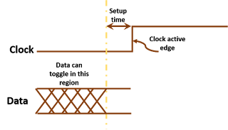
When setup time point is  before the arrival of clock edge, setup time is said to be positive.
Figure 1: Positive setup time


Zero setup time: When setup time point is at the same instant as clock's active edge, setup time is said to be zero. Figure 2 shows a situation wherein setup time is zero.
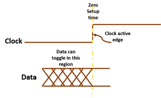
When setup time point is at the same instant as clock's active edge, setup time is said to be zero.
Figure 2: Zero setup time


Negative setup time: When setup time point occurs after clock edge, setup time is said to be negative. Figure 3 shows timing waveform for negative setup time.
When setup time point occurs after clock edge, setup time is said to be negative.
Figure 3: Negative setup time


What causes different values of setup time: We have discussed above theoretical aspects of positive, zero and negative setup time. Let us go a bit deeper into the details. Figure 4 shows a positive level-sensitive D-latch. As we know from the definition of setup time, setup time depends upon the relative arrival times of data and clock at input transmission gate (We have to ensure data has reached upto NodeD when clock reaches input transmission gate). Depending upon the relative arrival times of data and clock, setup time can be positive, zero or negative.
Figure 4: Positive level-sensitive latch
Let us assume the delay of an inverter is 1 ns. Then, to ensure that the data has reached NodeD when clock edge arrives at input transmission gate, data has to be available at the input transmission gate at least 2 ns before. So, if both data and clock reach the reference point at the same time, the latch has a setup time of 2 ns.

Now, if data takes 1 ns more than clock to reach input transmission gate from the reference point, then, data has to reach reference point at least 3 ns before clock reference point. In this case, setup time will be 3 ns.

Similarly, if data takes 1 ns less than clock to reach input transmission gate, setup time will be 1 ns. And if data takes 2 ns less than clock to reach input transmission gate, setup time will be zero.

Now, if there is further difference between delays of data and clock from respective reference points to input transmission gate, the hold time will become negative. For example, if data takes 3 ns less than clock to reach input transmission gate, setup time will be -1 ns.

This is how setup time depends upon relative delays of data and clock within the sequential element. And it completely makes sense to have negative setup time.

Also read:

Positive, negative and zero hold time


As we know from the definition of hold time, hold time is a point on time axis which restrains data from changing before it. Data can change only after hold time has elapsed. Now, there is no constraint on the occurrence of hold time point with respect to clock edge. It can either be after, before or at the same instant of time as that of clock active edge.

Posotive hold time: When hold time point is after the arrival of clock active edge, hold time is said to be positive hold time. Figure 1 below shows positive hold time.

Positive hold time, hold time, data can toggle after clock edge, data needs to be stable at least for hold time after clock edge
Figure 1: Positive hold time


Zero hold time: When hold time point is at the same time instant as that of clock active edge, we say that hold time of the sequential element is zero. Figure 2 below shows timing waveform for zero hold time.


Data can toggle right after clock edge
Figure 2: Zero hold time


Negative hold time: Similarly, when hold time point comes earlier on time scale as compared to data, we say that hold time of the sequential element is negative. Figure 3 shows timing waveform for negative hold time.

Negative hold time allows data to toggle even before clock ege
Figure 3: Negative hold time


We have discussed above theoretical aspects of positive, zero and negative hold time. Let us go a bit deeper into the details. Figure 4 shows a positive level-sensitive D-latch. As we know (from definition of hold time), hold time depends upon the relative arrival times of clock and data at the input transmission gate (We have to ensure data does not reach NodeC). Depending upon the times of arrival of clock and data, hold time can be positive or negative.

Figure 4: Positive level-sensitive D-latch

Let us say, the delay of an inverter is 1 ns. Then, we can afford the data to reach transmission gate input even 0.9 ns before arrival of clock at transmission gate. This will ensure data reaches NodeC (-0.9 + 1 =) 0.1 n after arrival of clock edge, if allowed. But, since, clock closes transmission gate, data will not reach NodeC. So, in this case, hold time is -1 ns. If the delay from NodeB to NodeC was something else, hold time would also have been different.

Now, if we say that clock arrives at transmission gate 1 ns earlier than data, then, by above logic, hold time of this latch will be -2 ns.

Similarly, if clock arrives at transmission gate 0.5 ns after data, hold time will be -0.5 ns.

And if clock arrive at transmission gate 1 ns after data, hold time will be  zero.

If the arrival time of clock is made more late, hold time will be greater than zero. For example, if arrival time of clock is 2 ns after data, hold time will be +1 ns.


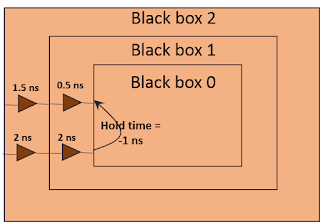
Hold time of the circuit is also dependent upon the reference point. For example, consider a multi-level black box as shown in figure 5. If we look at black box 0, its hold time is -1 ns. At level of black box 1, wherein clock travels 2 ns and data travels 0.5 ns to reach black box 0, hold time is (-1 + 2 - 0.5 = ) 0.5 ns. Similarly, at the level of black box 2, hold time is 1 ns. This is how, hold time depends upon the relative arrival times of clock and data. And it completely makes sense to have a negative hold time.

DFT basics

DFT stands for Design For Testification. DFT engineers try to make the testing of design more cost effective by introducing some structures into the design itself. By doing so, the overall test cost, and hence, cost of production comes down. Below, we list some of our posts covering the basics of DFT. Please provide your feedbacks regarding the topics you want to see as a part of this list. :-) Happy learning.

Setup time vs hold time

In digital designs, each and every sequential element has some restrictions related to the data with respect to clock in the form of windows in which data can change or not. There is always a region around the active edge of the clock in which data is not allowed to change at the input of the sequential element. This is because, if the data changes at the input within this window, we cannot guarantee the output. If this happens, there can be one of the three possibilities:
  • Current output data can be the result of current input data
  • Current output data can be the result of previous input data
  • The output can go metastable (as explained in metastability)
This region around clock edge is marked by two boundary lines, one perrtaining to setup time, and other to hold time. The region between these two lines is generally termed as setup-hold window. Figure 1 below shows the setup-hold window.
Figure 1: Figure showing setup/hold window of a sequential element
There are certain points of difference between setup time and hold time that we need to keep in mind:
  • Setup time signifies the point in time before which data needs to be stable, whereas hold time is the point of time after which the data needs to be stable
  • Adherence to setup time ensures that the data launched at previous active clock edge by another flip-flop gets captured at the current clock edge. On the other hand, adherence to hold time ensures that the data launched at the current edge does not get captured on the same edge.
  • Above point also means that setup time adherence ensures that the design goes to next state smoothly, whereas hold time adherence means the current state is not disturbed.
Hope this post helped you in understanding the basic difference in setup time and hold time.

Also read:

Propagation delay of a net

Definition of net propagation delay: The propagation delay of a net can be defined as the amount of time it takes a logic signal to propagate from the output of one logic gate to the input of another. Normally, it is defined as the difference between the times when the output of driver gate of net reaches 50% of its final value to when the input of the load cell of net reaches 50% of its final value.

How net delay is calculated: The net delay is calculated from the parasitics of the net. The parasitics are calculated based upon the topology of the net. These may also be read in from the parasitics file (SPEF, DSPF etc). The resulting RC-circuit resulting from the net topology is, then, simulated using certain algorithms (cosidering speed and accuracy requirements) for net delay.

Hold time

Definition of hold time: Hold time is defined as the minimum amount of time after arrival of clock's active edge so that it can be latched properly. In other words, each flip-flop (or any sequential element, in general) needs data to be stable for some time after arrival of clock edge such that it can reliably capture the data. This amount of time is known as hold time.

We can also link hold time with state transitions. We know that the data to be captured at the current clock edge was launched at previous clock edge by some other flip-flop. And the data launched at the current clock edge must be captured at the next edge. Adherence to hold time ensures that the data launched at current edge is not captured at the current clock edge. And the data launched at previous edge is captured and not disturbed by the one launched at current edge. In other words, hold time ensures that the current state of the design is not disturbed.

Figure 1 : Hold time


Figure 1 shows that data is allowed to toggle after the yellow dotted line. This yellow dotted line corresponds to hold time. The time difference between the active clock edge and this yellow dotted line is hold time. Data cannot toggle before this yellow dotted line for a duration known as setup-hold window. Occurrence of such an event is termed as hold violation. The consequence of such a violation can be capture of wrong data (better termed as hold check violation) or the sequential element going into meta-stable state (hold time violation).


Figure 2: A positive level-sensitive D-latch
Latch hold time: Figure 2 shows a positive level-sensitive latch. If there is a toggling of data at the latch input close to negative edge (while the latch is closing), there will be an uncertainty as if data will be capture reliably or not. For data to be captured reliably, next data must not reach Node C when closing edge of clock arrives at the input transmission gate. For this to happen, data must not travel NodeA -> NodeB -> NodeC before clock edge arrives. Data must change after this time interval only. 

Flip-flop hold time: Figure 3 below shows a master-slave negative edge-triggered D flip-flop using transmission gate latches. This is the most popular configuration of a flip-flop used in today's designs. Let us get into the details of hold time for this flip-flop. For this flip-flop to capture data reliably, new data must not be present at nodeD at the arrival of negative edge of clock. So, data must not travel NodeA -> NodeB -> NodeC -> NodeD when clock edge arrives. For data to not reach NodeD when clock edge arrives, it must toggle after some interval A with respect to clock. This interval corresponds to hold time of the flip-flop.We can also say that the hold time of flip-flop is, in a way, hold time of master latch.
 A D-type flip-flop consists of two latches connected back to back in master-slave format
Figure 3: D-flip flop

Hope this helped you in understanding the basics of hold time. You can suggest any improvement you think below in comments.

Setup and hold interview questions

Almost every interview for a VLSI design engineer has at least a question related to setup and hold. So, it is very important to prepare well. We list below a few topics related to setup and hold that may prove to be more than useful for setup and hold related interview questions.


Please share your interview experiences with us in comments so that these can be of help to other readers. Also, if you have any suggestion for us, you can get in touch with us. All the best. :-)

Liberty format : an introduction

What is liberty format: Liberty format is an industry standard format used to describe library cells of a particular technology. A cell could be a standard cell, IO Buffer, complex IP etc. Library cell description contains a lot of information like timing information, power estimation, other several attributes like area, functionality, operating condition etc. Speaking more technically, liberty format is a format to represent timing and power properties of black boxes (which we cant descend into). Liberty is an ASCII format, usually represented in a text file with extension ".lib". In this section, we will discuss timing aspects (delay and transition times) related to liberty format.

How is liberty file populated with data: The cells represented through liberty files are first simulated under a variety of conditions representative of actual design conditions that the cell may be exposed to. This process is known as characterization of library cells. As a very simple example, the delay of an inverter depends upon the input transition time and output load capacitance seen by it. The inverter will be characterized for a range of input transitions and output load capacitances. This characterization data, will then, be put into liberty in the form of a look-up table representing delay values at different transition times and load values.

To understand the different constructs related to timing in liberty file, let us take example of inverter. Rising transition at the input of inverter produces falling transition at the output of inverter and vice-versa. Hence there are two types of delay :

  1. Rise delay : It is the propagation delay (see definition) between output and input when output changes from 0 to 1.
  2. Output fall delay : It is the propagation delay between output and input when output is changing from 1 to 0.
In the real world, signal does not change its state from 0 to 1 or 1 to 0 abruptly. It takes some time to change its state. Hence, delay is measured based upon the threshold points. Threshold points in the liberty file are specified as below:


# threshold point of input falling edge
input_threshold_pct_fall : 50.0 ;

# threshold point of input rising edge
input_threshold_pct_rise : 50.0 ;

#threshold point of output falling edge
output_threshold_pct_fall : 50.0 ;

#threshold point of output rising edge
output_threshold_pct_rise : 50.0 ;


NOTE : these values are in percentage. e.g. If vdd is 5v then all of the above values will be 2.5.

So, Output rise delay is time difference between output_threshold_pct_rise and input_threshold_pct fall. Similarly Output fall delay is time difference between output_threshold_pct_fall and input_threshold_pct_rise.

Transition time : Time it takes for a signal to changes its state from one level to another level. Transition time is represented in terms of slew in liberty. Actually slew is inversely proportional to transition time. More the transition time, lesser is the slew rate and vice-versa. As we know that
voltage transition at the output is :
V = Vdd * [ 1 - e^ ( -t/(RC ) ) ] 

As Voltage equation is exponential, the voltage waveform is asymptotic at ends It is difficult to determine the exact start and end point of transition hence transition time is defined in terms of threshold values as follow :


# lower threshold point for falling  edge

slew_lower_threshold_pct_fall  : 30;

# upper threshold point for falling  edge
slew_upper_threshold_pct_fall : 30;

# lower threshold point for rising  edge
slew_lower_threshold_pct_rise : 70;

# upper threshold point for rising  edge
slew_upper_threshold_pct_rise : 70;