Does inserting lockup latch affect Logic Equivalence Check (LEC)

 Logic equivalence check is normally carried out to ensure some processing of the design (example logic synthesis) has not resulted in change of functionality. It flags any logical changes with respect to a golden set of collaterals. There are many applications of logic equivalence checking, some of the prevalent ones pertaining to:

1. Logic equivalence check between RTL and corresponding synthesized netlist to ensure the logic synthesis has not introduced any functional issues

2. Logic equivalence check between two sets of netlists after doing netlist edits. 


One thing to note here is that since RTL is the starting point here, LEC is done only for the logic present in the RTL, even for netlist vs netlist LEC (exceptions can be there). Other logic, such as scan chains are bypassed by application of certain constraints during LEC. For such logic, there are other methods to ensure correctness, such as scan tracing check to ensure there are no unintentional issues to trace scan chains.

Insertion of lockup latch also falls under non-functional netlist edits, hence not covered under LEC in normal scenarios. We must observe that fanout if lockup latch goes to scan_in pin of flop, which is not checked under LEC.

Analogy between English and C as a language

In our first post, we discussed that any programming language is a language in the first place. So it must be analogous to a language in how the constructs are used and formed in it. In this post, we will try to understand this aspect by making analogous comparison between English and C as a programming language.

As we know that any language has its character set as the most basic construct. English has Roman script as its character set, which includes a-z, A-Z. Similarly, to write a program in any programming language, you must be aware of the character set of that programming language.


The character set of C language is following:

– Alphabets (a-z, A-Z)

– digits (0-9)

– special symbols (any printable symbol like !,&,@,#) etc


In other words, any thing that can be printed forms the character set of C language. You can use these to form bigger constructs that we will discuss later.


Next, we know that in English, characters combine to make words, which have specific meanings. And these words may be of different categories viz nouns, pronouns, adjectives, adverbs etc. On a similar note, in C, we have variables, constants and keywords.


Similar to words combining to form sentences, C has commands/instructions. These instructions carry specific meanings and usually are related to either some task to do for the computer, or some message for the user.


Next in hierarchy, we have paragraphs or essays in English. On a similar note, we have programs in C that carry out a task on a whole. For instance, we might have a program to create a database which is a combination of multiple instructions.


Thus we have discussed how C is analogous to English, or any other language in terms of the constructs. I am pasting below the link of video from my YouTube channel in Hindi. You can go through it if you wish to.


Starting with C programming language

Before we start discussing about C as a programming language, we must be clear about the term programming language itself. Only then, we will be able to appreciate C as a programming language.

As the name suggests, programming language is a language. A language that computer understands, and that is used to interact with the heart of the computer. Obviously this language has to be understood by programmers as well, so that the interaction is understood by both the parties. In other words, through a programming language, you are giving instructions to the computer on the tasks it has to perform.


How programming language enables you to interact with computer is a bigger question. A computer does not directly understands the programming language, it understand only electrical signals (high voltage and low voltage, or in simpler terms 0 and 1, also called machine language). Although humans can interpret this coded language, but it is very inefficient and error prone. So we need a translator that converts this series of 0s and 1s into human readable version, the software that does this job is called a compiler or an interpreter based upon the method of translation used. C and other high level languages such as Java, Visual Basic etc are compiled languages, meaning that compiler is the heart of these languages. There are many compilers available for each programming language, for example C has turboC and GCC as compilers. You can understand these as products of different companies, which differ in their characteristics, services and ease of use they provide. But their basic task is to convert C code into computer under-standable 0s and 1s.


For our journey of talking about the basics of C, we will be using an online compiler programiz.com. I personally prefer online compilers because of the obvious benefits they provide; for example, you can access your code from multiple devices. You can use any compiler you wish, or you can use any other compiler as well.


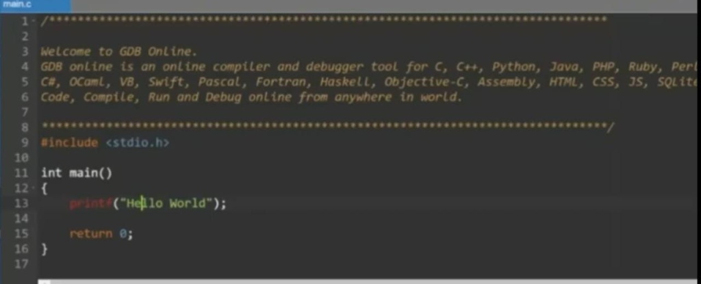
Most of the online compilers provide you with an option to have a pre written code segment, which you can use as a start point for your program. For instance, onlinegdb.com compiler gets you started with a default “Hello world!” printing program. Which you can modify as per your need. Typically, the first program anyone learns to execute in any programming language is to print hello world. We will also use the same to learn basic programming constructs of C language.


Program to print “hello world” in C language


If you see the screenshot above, a typical C program has following constructs:


1. #include section: This section is used to include pre compiled C libraries to your code. These are already available C programs in machine language, to perform specific tasks. For example, studio.h enables you to get input from standard terminal and output to standard terminal as well.


2. Main() section: This is where the execution of a C program starts. Whatever your programs does has to be written directly or indirectly into this section (we will discuss more on this later). For instance, the statement printf is to display on screen, whatever is written within the double quotes. So, when this program executes, “Hello world” will be displayed on the screen.


So that concludes our first post, I hope we will have fun time learning C together. I am pasting below the video link from my YouTube channel in Hindi. You can go through it, if you wish to.


Welcome to glittering code

Hi there, I am a software professional with over a decade of industry experience. I am here to share my knowledge and experience with all of you, and in the process, learn a lot of things myself. As the saying goes, a good code is all that glitters. Let’s begin our journey to make our codes glitter.

How to interpret default setup and hold checks

In the post "setup and hold checks", we discussed the meaning and interpretation of setup and hold checks. We also discussed the terms "default setup check" and "non-default setup check" and same for hold checks. Essentially, every timing check, be it setup/hold check, data check or clock gating check follows a default edge-relationship depending upon the types of elements involved. For instance, default setup check or setup timing path from a positive edge-triggered flip-flop to a positive edge-triggered flip-flop is full cycle, whereas hold check path is zero cycle. Have you ever thought why is default behavior like this in case of setup and hold checks. Most of us find the setup and hold check interpretation confusing for many cases which are not straightforward, such as positive level-sensitive latch to positive level-sensitive latch timing path. And we believe what the STA tools show us in terms of setup and hold checks. In this post, we will discuss how we can demystify the edge-relationship for setup and hold checks.

For this, we need to understand state machine behavior. Each state of an FSM can be interpreted as an instant of time, and setup check is a bridge between two states of the FSM allowing smooth transition from one state to the next. Every opportunity to alter state machine can be interpreted as one state. For instance, for a state machine comprising only positive edge-triggered flip-flops, every positive edge of clock can be interpreted as a state. Similarly, for a state-machine comprising both positive edge-triggered and negative edge-triggered elements, each (positive or negative) edge is a state. Now, coming to level-sensitive elements, their capturing instant is spread over a time interval rather than being an edge. For example, a positive latch can capture data at any time between positive edge and negative edge. Thus, for a design comprising all kinds of level-sensitive and edge-sensitive elements, the states of the FSM mapped to time should look like as shown in figure 1.

Figure 1: State machine behavior of a generic design

The FSM behavior shown in figure 1 is in line with commonly understood default FSM behavior. The default setup and hold checks, which are a way of transitioning to adjacent next state, also function the same way. In other words, default behavior of simulation and timing tools is in line with figure 1. It is, of course, possible to design FSMs that do not follow figure 1 through introduction of multi-cycle paths, but if not specified manually, figure 1 is followed.

We will now discuss a rule that will help you to figure out default setup/hold checks between all sequential element types.

Rule for default setup check: The very next instant that the data can be captured right after it has been launched, forms the default setup check. For instance, consider a positive edge-triggered flip-flop launching data at T=10 ns, which is to be captured at another flip-flop with clock waveform as shown below (for both launch and capture elements). After T=10ns, the next instant that will capture the data at each type of flop and latch (either positive or negative) is given in figure 2.


Figure 2: Data capturing instances for different sequential element types

Thus, post 10 ns, a positive latch can capture at any instant of time between 10 ns and 15 ns, negative latch can capture the data at any instant between 15 ns and 20 ns; a positive flop will capture the data at 20 ns and a negative flop will capture data at 15 ns. These all form default setup check. The previous such instant that the data could have been captured forms the default hold check. For instance, for positive flop, the instant before 20 ns that could have captured the data is 10 ns itself. Similarly, for negative flop, hold check is at previous negative edge (10 ns launch -> 5ns capture). For positive latch, hold check is also the same as negative flop  (10 ns launch -> 5ns capture) and for negative latch, hold check is same as for positive flop (10 ns launch -> 10 ns capture).

In the below posts, we discuss default setup and hold checks for different elements and for different clock ratios. I hope it covers all. Please let me know for any feedback through comments or email (myblogvlsiuniverse@gmail.com).


Default Setup/hold checks - positive flop to negative flop timing paths

The launch/capture event of a positive edge-triggered flip-flop happens on every positive edge of the clock, whereas that of a negative edge-triggered flip-flop occurs on the negative edge of the flip-flop. In this post, we will discuss the default setup/hold checks different cases - same clock, 1:n clock ratio clock and n:1 ratio clock. And this should cover all the possible cases of setup/hold checks.

Case 1: Both flip-flops getting same clock

Figure 1: Pos-flop to neg-flop default setup/hold checks when clocks are equal in frequency

Figure 1 shows a timing path from a positive edge-triggered flip-flop to a negative edge-triggered flip-flop. Let us say the data is launched at instant of time "T", which is a positive edge. Then, the next negative edge following time "T" serves as the edge which captures this data; thus forming the default setup check. And the very previous negative edge serves as the hold check. This is shown in the first part of figure 1. Thus, in this case, both setup and hold checks are half cycle.

Setup and hold slack equations

Setup slack = Period(clk)/2 + Tskew - Tclk_q - Tcomb - Tsetup

Hold slack = Period(clk)/2 + Tclk_q + Tcomb - Tskew - Thold


Case 2: Flip-flops getting clocks with frequency ratio N:1 and positive edge of launch clock coincides with negative edge of capture clock

One of the cases where this happens is when clock is divided by an even number. Another is when odd division is followed by inversion. The resulting waveform will be as shown in figure 2. In this case, each positive edge of launch flip-flop is capable of launching a fresh data, but will be overwritten by next data. Only the one which is launched on the positive edge closest to the negative edge of capture clock will get captured at the endpoint. Similarly, the data which is launched at the edge coinciding negative edge of capture clock must not overwrite the data captured at the same edge. The setup and hold checks, thus formed, are as shown in figure 2 below. The setup check is full cycle of launch clock, whereas hold check is a zero cycle check.


Figure 2: Default setup/hold checks for case 2

Setup and hold slack equations

Setup slack = period(launch_clock) + Tskew - Tclk_q - Tcomb - Tsetup

 Hold slack = Tclk_q + Tcomb - Tskew - Thold


Case 3: Flip-flops gettings clocks with frequency ration N:1 and positive edge of launch clock coincides with positive edge of capture clock

One of the cases where this happens is when capture of the data happens on an odd divided clock. The resulting setup and hold checks are as shown in figure 3. Both setup and hold checks are half cycle of faster launch clock.

Figure 3: Default setup/hold checks for case 3
Setup and hold slack equations

Setup slack = period(launch_clock)/2 + Tskew - Tclk_q - Tcomb - Tsetup

 Hold slack =  period(launch_clock)/2 + Tclk_q + Tcomb - Tskew - Thold

Case 4: Flip-flops getting clocks with frequency 1:N and positive edge of launch clock coincides with negative edge of capture clock

One of the cases is when division is performed after inversion of the master clock and data is launched on the divided clock. Figure 4 shows the default setup/hold checks for this case. In this case, setup check is equal to full cycle of faster clock and hold check is a zero cycle check.

Figure 4: Default setup/hold checks for case 4
Setup and hold slack equations

Setup slack = period(capture_clock) + Tskew - Tclk_q - Tcomb - Tsetup

 Hold slack = Tclk_q + Tcomb - Tskew - Thold

Case 5: Flip-flops getting clocks with frequency 1:N and positve edge of launch clock coincides with positive edge of capture clock

This is a case of even division, or inversion, followed by odd division, followed by inversion. The setup and hold checks, both are equal to half cycle of faster clock.

Setup and hold slack equations

Setup slack = period(capture_clock)/2 + Tskew - Tclk_q - Tcomb - Tsetup

 Hold slack =  period(capture_clock)/2 + Tclk_q + Tcomb - Tskew - Thold

Can you think of any other scenario of setup/hold checks for this case? Please feel free to share your views.

Clock relationship between reset synchronizer and fanout flip-flops

As we know, all flip-flops which are required to be "out of reset" at the same time are placed in fanout of a single reset synchronizer. In this post, we will discuss if there is any relationship required between clock frequency of reset synchronizer and the clock frequency of the flip-flops in fanout. For now, let us assume that all the flip-flops in the fanout of reset synchronizer work on a single clock "CLK". <dsfdsf> discussed the case when the flip-flops are working on multiple clocks.

Let us first assume that reset synchronizer's clock period is N*CLK_PERIOD; i.e. reset synchronizer gets a DIVIDE_BY_N clock of the flip-flops' clock. Figure 1 below shows the setup check from a clock with period N*CLK_PERIOD to a clock with period CLK_PERIOD. Since, all the flip-flops have same setup check being formed, all will get out of reset at the same edge; thus, fulfilling the requirement.


Similarly, there is a definite setup check from a clock with period CLK_PERIOD/N to a clock with period CLK_PERIOD as shown in figure 2 below. Thus, if reset synchronizer works on clock with frequency "N" times the flip-flops in fanout, we get all the flip-flops out of reset at same time, thereby, fulfilling the requirement again.


Thus, we see that if all the flip-flops in fanout of reset synchronizer work on a single clock, there is no relationship required between frequency of reset synchronizer and frequency of fanout flip-flops as long as we meet the setup and hold requierements.   However, this is not true when flip-flops work on multiple clocks as discussed in <SDFDSF>.


Design problem: Reset synchronizer clock for multi-frequency flip-flops in fanout

Design problem: A set of flip-flops, some working on 100 MHz clock and others working on 200 MHz clock are required to come out of reset together. What should be the clock of reset synchronizer

Solution: Since all the flip-flops are required to come out of reset in the same cycle, all these must get reset from a single reset synchronizer. Now, as the question states that the flip-flops in the fanout of reset synchronizer are working on two clocks. We need to find the correct-by-design clock that reset synchronizer should be working on. Let us assume that the correct clock to be connected to reset synchronizer is one of the two frequencies given.

Figure 1: Reset synchronizer


First, let us check by assuming that reset synchronizer works on positive edge of 100 MHz clock. Figure 2 shows the setup checks for 100 MHz -> 100 MHz and 100 MHz -> 200 MHz paths. Let us say, reset deassertion propagates to R1/Q at edge (1). Going by figure 2, all flip-flops working on 200 MHz clock will be out of reset at edge (3) and all flop-flops working on 100 MHz will be out of reset at edge (5). Thus, reset synchronizer working on positive edge of 100 MHz clock does not solve our purpose.

Figure 2: Reset synchronizer works on positive edge of 100 MHz clock


Now, let us check the same when reset synchronizer works on positive edge of 200 MHz clock. In this case, reset can deassert either on edge (1) or edge (3). If reset deasserts on edge 3, then, we have both the categories of flops coming out of reset at same time edge (5). But if reset deasserts on edge (1), both categories of flops get out of reset at different times. Thus, we can get the reset synchronizer working on 200 MHz clock, but we have to ensure by design that reset gets deasserted on the edge of 200 MHz clock that coincides with negative edge of 100 MHz clock. Figure 3 and figure 4 discuss these scenarios.

Figure 3: Reset synchronizer works on positive edge of 200 MHz clock coinciding with positive edge of 100 MHz clock


Figure 4: Reset synchronizer works on positive edge of 200 MHz clock coinciding with negative edge of 100 MHz clock

Same scenarios are expected as figure 3 & 4 when we make reset synchronizer work on negative edge of 200 MHz clock.

Now, let us explore the last option; i.e., reset synchronizer working on negative edge of 100 MHz clock. In this case, as shown in figure 5, both 100 MHz and 200 MHz flip-flops come out of reset on same edge. Thus, this case works perfectly. Figure 5 illustrates this.

Figure 5: Reset synchronizer works on negative edge of 100 MHz clock


Can you provide any other solution that is possible and better than ones discussed here.

Data check timing paths

Data check is a timing check, either picked from timing model or user-defined, between two related data signals. Thus, data check timing path is a timing path, wherein both reference signal and constrained signal are data signals launched by same or related clocks. Figure 1 below shows an example data check path where both signals are launched from positive edge-triggered flip-flops. Based upon the type of check being formed (data setup check or data hold check), we can categorize these as data-setup-check path or data-hold-check path.


Constraining data-check timing paths: To constrain data-check timing paths, we first need to ensure that there is a data-check associated with the signals in question. It can either be defined in the timing model being picked or we can define using SDC construct "set_data_check". Once data check is defined, we can simply ensure that both the reference signal and constrained signal are launched from same clock or related clock to see data-check timing path reported.


Clock gating timing paths

A timing path falls under the category of clock gating timing paths, when:

  1. The endpoint is the "EN" pin of Integrated Clock Gating (ICG) cell   OR
  2. The endpoint is one of the input pins of a combinational cells with at least one of the other pins getting a clock signal
The motive behind a clock gating timing path being treated as a constrained path is to constrain the path in such a way that there is no glitch or metastability observed at the output of the gate. In other words, either the output of the gate transmits complete pulses of clock; or it does not transmit any signal at all. The max and min checks in case of clock gating paths are called as "clock gating setup check" and "clock gating hold checks". The startpoint for these paths can be any of input port or a sequential element. Figure 1 below shows a few examples of clock gating timing paths.


Constraining clock gating check timing paths: As explained in clock gating checks, there are two types of clock gating checks - one which require data at the endpoint to change when clock is low (AND-type check) and vice-versa (OR-type check). There are scenarios when STA tool is able to recognize the type of check being formed. This happens when the endpoint is a simple gate such as AND or OR gate. In that case, by default, these are constrained as clock gating endpoints. The only thing we have to do is to ensure that proper clock signals reach the startpoint and the endpoint. But there are scenarios when the gate is complex and it is not possible for STA tool to differentiate which of the two types of checks should be formed. In those cases, these are not by-default constrained. And we have to specifically ask the STA tool to treat these as clock gating endpoints by using "set_clock_gating_check" SDC command, in addition to defining proper clocks.

Why is the sum of setup time and hold time always positive

In our post "Setup and hold - origin", we discussed that every device captures data within a certain window known as "setup + hold window". During this time, data must be held stable so that it can be captured properly. Outside this window, data is allowed to toggle.


Figure above shows "setup+hold window". This window is characterized by the setup and hold times of the device. The width of this window is essentially the sum of setup time and hold time. Thus, if the sum of setup and hold time is positive, it means there is a finite window wherein the device is allowed to capture the data. On the other hand, a negative sum of setup time and hold time indicates that the width of this window is negative. In other words, the window does not exist. So, a negative setup and hold time implies that the device cannot capture the data at all!! 

Thus, for a functional device, we always need the sum of setup and hold times to be positive. :-)

Reg-to-out paths

A reg-to-out path has a sequential element as the "startpoint" and an output port as "endpoint". We can categorize reg-to-out paths as flop-to-out and latch-to-out, but this differentiation is not widely prevalent. Figure 1 below shows a reg-to-out path originating from a positive edge-triggered flip-flop.


The output port as an "endpoint" is modeled as an alternative of a flip-flop capturing data outside. The SDC command for doing so is "set_output_delay". It represents the portion of data path and clock skew outside the design. Also, we have not shown the clock path in the above figure. The clock source may be situated inside the design and provide clock to outside sitting flip-flop (more commonly called as master transmit or clock-out-data-out in I/O protocol jargon). Or it may be situated outside, thereby, sending data to internal flip-flop through another port (commonly called as clock-in-data-out or slave transmit mode in I/O protocol jargon). Both these scenarios are shown in figures 2 and 3 below.


Constraining reg-to-out paths: As we discussed earlier also, we model the data path and clock path that is not visible inside the design for reg-to-out paths using "set_output_delay" command. There are two cases for constraining output ports:

Case 1: Constraining with respect to virtual clock
Constraining with virtual clock is helpful when we know that the data-path budgeting is exclusive of clock path, for instance, a sub-design of an SoC. A virtual clock is a clock without any source. So, data-path outside the block can be modeled using "set_output_delay" with respect to virtual clock and clock path outside the block can be modeled using "set_clock_latency" for virtual clock. The steps are listed below:

  • "create_clock" at clock source : CLK
  • "create_clock" without a clock source : VCLK (virtual clock)
  • set_output_delay at output port with respect to VCLK

Case 2: Constraining with respect to real clock

When we know that the outside data path delay and clock path delay are fixed, then we can constrain the port with respect to real clock itself. The steps are listed below:

  • "create_clock" at clock source : CLK
  • "set_output_delay" at output_port with respect to CLK (or with respect to a clock related to CLK) 

In-to-reg paths

An in-to-reg path has an input port as "startpoint" and a sequential element as the "endpoint". Similar to reg-to-reg paths, we can categorize these into in-to-flop and in-to-latch paths; but this differentiation is not prevalent widely. Figure 1 below shows a sample in-to-reg path ending at a positive edge-triggered flip-flop.


The input port as a startpoint is modelled as an alternative of a flip-flop launching data from the outside. The SDC command for doing so is "set_input_delay". It represents the portion of total clock period and clock skew that is outside the design. Also, we have not shown the clock source in the above figure. The clock source may be situated inside the design and provide clock to the outside sitting flip-flop (more popularly called as clock-out-data-in or master receive mode in terms of I/O protocol jargon). Or it may be situated outside, thereby sending clock signal to the internal flip-flop through another port (more popularly called as clock-in-data-in or slave receive mode in I/O protocol jargon). Both these scenarios are shown in figures 2 and 3 below.

Figure 2


Figure 3


Constraining in-to-reg paths: As we discussed earlier, we model the data-path and clock-path that is not visible inside the design for in-to-reg paths. This is done using "set_input_delay" command. There are two cases for constraining input ports:

Case 1: Constraining with respect to virtual clock
Constraining with virtual clock is helpful when we know that the data-path budgeting is exclusive of clock path, for instance, a sub-design of an SoC. A virtual clock is a clock without any source. So, data-path outside the block can be modelled with "set_input_delay" with respect to virtual clock and clock path outside the block can be modeled using "set_clock_latency" for virtual clock. The steps are listed below:

  • "create_clock" at clock source
  • "create_clock" without any source (virtual clock)
  • set_input_delay at input_port with respect to virtual clock created 

Case 2: Constraining with respect to real clock
When we know that the outside data path delay and clock path delay are fixed, then we constrain the input port with respect to real clock itself. An example is SoC level protocol signals such as ethernet signals.  The input port is constrained either with respect to the same clock going to the endpoint or some clock related to it. The steps are listed below:

  • "create_clock" CLK at clock source
  • "set_input_delay" at input_port with respect to CLK (or with respect to a generated_clock created from the CLK

Reg-to-reg paths

In a reg-to-reg path, both startpoint and endpoint are sequential elements; i.e. either an edge-triggered element or a level sensitive element. Edge-triggered elements are mostly flip-flops, memories or edge-triggered arcs of sub-partitions of the design. Level sensitive elements are mostly latches or any such element such as a sub-partitions level sensitive arcs. Edge-triggered elements can be commonly referred as flops as far as our scope is concerned. Similarly, level-sensitive elements can be referred to as latches.

Reg-to-reg timing paths can be broadly categorized into four categories depending upon if the startpoint and endpoint is level-triggered or edge-sensitive:
  • Latch-to-latch paths: Both startpoint and endpoint are level-sensitive. See setup and hold checks for latch-to-latch paths


Common characteristics of reg-to-reg paths:
  • All the components of a timing path we discussed in timing paths, i.e. startpoint, endpoint, launch clock path, capture clock path and data path exist for a reg-to-reg path.
  • To constrain reg-to-reg paths, we just have to ensure that both the startpoint and endpoint receive a valid clock signal and there is no timing exception (such as false path between the clocks) masking the timing path.

Timing path types

In the post - timing paths- we discussed about timing paths and common components of a timing path. We also discussed that the type of a timing path is perceived by its components, the elements encountered in reference path, the elements encountered in constrained path and the type of check between reference signal and constrained signal. We also discussed how these signal traversals are differentiated into different components of timing paths - startpoint, endpoint, launch clock path and capture clock path. Based on these, we can categorize the timing paths into broadly following categories. We will not talk about min/hold and max/setup paths, but each of below categories can further be differentiated into these based upon the type of check being formed. Also, it is to be noted that every timing path is, essentially, either of the type of a generic timing path or a modeling in some or the other form of  a generic timing path as shown in figure 1.

Figure 1: Generic timing path


Reg-to-reg paths: The timing path where both "startpoint" and "endpoint" are sequential elements, e.g. a flip-flop, a latch or a memory element is termed as a reg-to-reg path in common terminology. 

In-to-reg path: The timing path where "startpoint" is an input port and "endpoint" is a sequential element, is termed as in-to-reg path.

Reg-to-out path: Here, "startpoint" is a sequential element and "endpoint" is an output port.

In-to-out path: In this type of path, "startpoint" is an input port and "endpoint" is and output port.

Clock gating paths: In this type of path, "startpoint" can be any out of sequential element, input port or output port. The endpoint is usually input pin of either a combinational gate or an Integrated Clock Gating cell (ICG). The common scenario involved is to time the arrival of constrained signal (termed as enable in clock gating paths) such that complete pulses of clock as reference signal are transmitted and there is no glitch at the output of the "endpoint".

Min-pulse-width-check paths: Here, both reference and constrained path, both are clock paths and common right from source till "endpoint". This type of path compares the latest arrival of rise transition of the clock with respect to the earliest arrival of fall transition of clock and vice-versa. The nature of check is max check only.

Data check paths: In this type of paths, both reference signal and constrained signal are data launched by a clock signal.

Point-to-point paths: The paths with only constrained signal are called as point-to-point paths. "startpoint" as well "endpoint" can be any sequential or combinational pin or port.

Timing paths

The most important element of a design in Static Timing Analysis is a timing path. A design is broken down into a set of timing paths. Each timing path is analyzed by a set of timing equations for possible violations of timing. A timing path can be defined as flow of timing information (such as delay, transition etc.) through a set of elements which can be accumulated and verified against a specified set of rules.

 A timing path can be supposed to be consisting of two sub-paths - a reference path through which reference signal traverses and a constrained path through which constrained signal traverses. Both of these essentially originate from same source (or have a definite relationship at their respective sources). At the terminal end of both, there is a relationship governing the arrival of constrained signal to the arrival of reference signal. Depending upon the type of reference signal and constrained signal, the type of elements encountered by these and the check that is formed between the two, we govern the type of path. For instance, in a reg-to-reg setup path, the reference signal is clock, constrained signal is data launched from a clock and traversing through a flip-flop and the check that is formed between the two signals is a setup check at a flip-flop as the endpoint.

Figure 1: Generic timing path in STA
Figure 1 above shows a generic timing path. The elements of the path are not shown individually. The path that is common among constrained signal and reference signal is termed as common path.

Based upon type of check being formed between constrained signal and reference signal, there are commonly two types of paths that are formed: max path/setup check path and hold check path/min path.

Max/setup check path: In this kind of path, the earliest arrival of reference signal and latest arrival of constrained signal is considered. The kind of check is known as setup check in most of the cases. And the type of path is called setup path/max path.

Min/hold check path: In this kind of paths, the earliest arrival of constrained signal and the latest arrival of reference signal is considered. The kind of check is known as hold check in most of the cases. And the type of path is called hold path/min path.

Let us move to the commonly perceived understanding of a timing path by taking an example of a reg-to-reg path. Figure 1 below shows an example of a timing path, which starts from a flip-flop and ends at a flip-flop.

Figure 2: Components of a reg-to-reg path


The above timing path (or any timing path, in general), has following components:

Startpoint: The element from which the data gets launched is known as startpoint. In general, it can be a sequential element (latch, flip-flop) or an input port. In case it is a flip-flop, the clock pin of the flip-flop is counted as the startpoint of timing path. For point-to-point paths, it can also be a combinational input or output pin.

Endpoint: The element at which timing path ends is called the endpoint. It can be data pin of flip-flop or an output port. For point-to-point paths, it can also be a combinational input or output pin.

Clock: Most of the timing paths are constrained by a clock signal, which clocks both startpoint and endpoint. The properties of the clock signal, such as clock period, jitter etc are defined in timing constraints.

Launch clock path: It refers to the path traversed by clock signal from clock source to the startpoint.

Capture clock path: It refers to the path traversed by clock signal from clock source to the endpoint.

Data path: It refers to the path traversed by data signal from starptoint to endpoint.

In the above example, launch clock path and data path together constitute constrained signal path and capture clock path constitutes reference signal path.

Timing requirements/constraints related to a reset synchronizer

In the post reset synchronizer, we discussed the functionality associated with a reset synchronizer.  Here, we will discuss the timing associated with a reset synchronizer. Figure 1 below shows a reset synchronizer.

Figure 1: Reset synchronizer

As we can see, a reset synchronizer is expected to have 3 pins other than a clock pin. We will discuss the timing requirements of each of these one-by-one:

  1. R0/D (Data input pin) is tied to 1, hence, no timing requirement related to this.
  2. Reset deassertion timing is required for R0/Q -> R1/D at the clock frequency at which reset deassertion is happening
  3. Similarly, reset deassertion timing is required for R1/Q -> functional_flops/Rbar pins
  4. Timing at R0/Rbar pin is not required, since, it is put there to absorb metastability and come out of metastability before next clock edge
  5. Timing at R1/Rbar pin is not required, since, when Rbar gets deasserted, R1/D and R1/Q are both at value "0".
  6. Both R0 & R1 need at least a certain pulse width at Rbar pin in order to detect the reset. This requirement is generally given in the timing model of flip-flop

Points 4 & 5 assume that there is not much skew between R0/Rbar and R1/Rbar, which is true since either there is a custom cell made as a reset synchronizer or both the flip-flops are placed very close to each other, leaving almost no scope for a large skew.

Points 2 & 3 require that reset synchronizer and its fanout flip-flops are clocked on a related clock.

Thus, there are following constraints related to a reset synchronizer:
  • Reset synchronizer must be clocked on either same or related clock to its fanout flops
  • set_false_path -to R0/Rbar
  • set_false_path -to R1/Rbar
  • Min-pulse-width requirement at Rbar pins modelled in timing models

Min-pulse-width-check timing paths

All sequential elements require the clock pulse to have a pulse of at-least a certain width in order to function correctly. This is coded in their timing models in terms of a "minimum pulse width" requirement. And the timing path pertaining to check minimum pulse width of a signal is termed as "min-pulse-width-check" timing path. A min-pulse-width-check timing path essentially checks the arrival of one transition of the clock at the endpoint with respect to its fall transition. In other words, both constrained signal and reference signal are the same, just the opposite transitions.

For instance, min-pulse-width-check timing path for a high pulse will have fall transition as the reference signal and rise transition as constrained signal. The latest arrival of rise transition is checked against earliest arrival of fall transition Similarly, min-pulse-width-check timing path for a low pulse will have fall transition as constrained signal and rise transition as reference signal. The latest arrival of fall transition will be checked against earliest arrival of rise transition.

Constraining min-pulse-width-check timing paths: There are two kind of scenarios:
  • Min-pulse-width requirement for the pin is picked from timing model
  • User specifically specifies a "min-pulse-width" check at a specific pin using "set_min_pulse_width" command. This may be required in certain scenarios, such as a clock going out of the design through an output port, and we need to maintain a minimum duty cycle for the outgoing clock.
Regardless of this, we just need to define a clock of required period and we can report min-pulse-width-check timing path as desired.

In-to-out paths

In-to-out paths start from an input port and end at an output port. Figure 1 below shows an in-to-out path. As shown in figure 1, most of the times (not always), in-to-out paths are subset of a reg-to-reg path seen from a higher level of hierarchy. For instance, an in-to-out path at the level of a block-level design may be a reg-to-reg path as seen at SoC flat.


For in-to-out paths, the clock path is always assumed fully outside the design. 

Constraining in-to-out paths: There are two ways that we can constrain in-to-out paths:

Constraining with respect to a virtual clock: We can consider in-to-out path as a sub-segment of a larger reg-to-reg path. And we can constrain these paths using a virtual clock. Using "set_input_delay" for input port and "set_output_delay" for output port with respect to same virtual clock, these paths can be constrained.
  • Create a clock VCLK without any source
  • "set_input_delay" at input_port with respect to VCLK
  • "set_output_delay" at output_port with respct to VCLK

Constraining as point-to-point paths: We can constrain in-to-out paths using "set_max_delay" command as point-to-point paths. However, using this approach, we may need to apply some extra constraints as well depending upon the behavior of the tool we are using.


Where does STA fit in backend design flow

Static Timing Analysis (STA) is an integral part of backend design cycle. At each stage in the design cycle, it is imperative to check for timing violations by carrying out static timing analysis and do course correction, if required. A typical physical design cycle involves logic synthesis followed by test insertion, placement, clock tree synthesis and data routing. At each of these stages, we need to ensure that the timing is under control by running STA. Figure 1 below shows, on a higher level, different steps involved in physical design cycle; and how STA is an integral part of each of the stages.

Figure 1: STA as an integral part of physical design cycle

The first step in physical design cycle is synthesis and test insertion followed by floorplanning and placement. Although, nowadays, some tools combine synthesis and placement to save on run time and efforts. At this level, STA is run with ideal clocks and estimated parasitic values either on the basis of fanout with a model known popularly as WLM (Wire Load model) or on the basis of actual placement of instances. Since, a lot of variables are not taken into account at this stage, it is preferred to meet setup timing with some margin so as to accommodate the degradation in setup timing due to those variables later in the design cycle. These variables include clock skew, uncommon path in clock network, data nets detouring during actual routing and crosstalk effects. When clock tree is built, we have actual clock skew numbers. So, STA needs to be run to check if the margins for clock skew need to be accommodated into some more optimization (area, power or timing) due to actual clock skews and uncommon clock paths being different than the margin assumed. Similarly, after data routing, we can run STA with actual parasitic values and crosstalk effects, thereby signing off timing using STA by running accross all possible corner scenarios.