Timing Corners – dimensions in timing signoff


Integrated circuits are designed to work for a range of temperatures and voltages, and not just for a single temperature and voltage. These have to work under different environmental conditions and different electrical setup and user environments. For instance, the temperature in the internals of an automobile may reach as high as 150 degrees while operating. Also, automobiles may have to work in colder regions where temperatures may reach -40 degrees during winters. So, a chip designed for automobiles has to be designed so as to be able to work in temperatures ranging from -40 to 150 degree Celsius. On the other hand, consumer electronics may have to work in the range of -20 to +40 degrees only. Thus, depending upon the application, the chip has to be robust enough to handle varying surrounding temperatures. Not just surrounding temperatures, the voltage supplied by the voltage source may vary. The battery may have an output voltage range. Also, the voltage regulator sitting inside or outside the chip may have some inaccuracy range defined. Let us say, a SoC has a nominal operating voltage of 1.2V with 10% variation. Thus, it can operate at any voltage from 1.08 V to 1.32V. The integrated circuits have to be tolerable enough to handle these variations. Not just these variations, the process by which the integrated circuits are manufactured has variations due to its micro nature. For example, while performing etching, the depth of etching may vary from wafer to wafer, and from die to die. Similarly, doping, width of wires drawn, distance between wires may vary for each wire from chip-to-chip. Depending upon these, the behavior (delay, static and dynamic power consumption etc) of cells on chip vary. These variations are together referred as PVT (Process Voltage Temperature) variations. The behavior of the devices also varies according to the PVT variations. The library (liberty) models of the cells are characterized for cell delays, transitions, static and dynamic power corresponding to different PVT combinations. Not just for cells, for nets too, these variations are possible. The net parameters (resistance, capacitance and inductance) may also vary. These parameters also account for cell delay. In addition, nets introduce delay of their own too. Hence, one may get nets with high or less delay. So, these variations also have to be taken into account for robust integrated circuit manufacture. This variation in net characteristic can be modeled as their RC variation as it accounts for changes in resistance and capacitance (ignoring inductance) of net.

The operating conditions of an SoC may vary based upon the application. For instance, an SoC being used in a car can be exposed to temperatures ranging from -40 to 150 degree celsius. The figure shows a racing car.

Figure 1: A racing car. (Taken from en.wikipedia.com)

With proper techniques, the patterns of the variations for both the cell and net parameters (delay, power, resistance and capacitance) are characterized and their minima and maxima are recorded. Each minima and maxima can be termed as a corner. Let us say, each minima/maxima in cell characteristics as ‘PVT corner’ and net characteristics as ‘extraction corner’.  Each combination of PVT extraction corners is referred to as a ‘timing corner’ as it represents a point where timing will be extreme. There is an assumption that if the setup and hold conditions are met for the design at these corners, these will be met at intermediate points and it will be safe to run under all conditions. This is true in most of the cases, not always. There is always a trade-off between number of signed-off corners and the sign-off quality.
 
For bigger technologies, say 250 nm, only two corners used to be sufficient, one that showed maximum cell delay and the other that showed least cell delay. Net variations could be ignored for such technologies. In all, there used to be 2 PVT and 1 extraction corner.  As we go down technology nodes, net variations start coming into picture. Also, cell characteristics do not show a linear behavior. Therefore, there is increased number of PVT as well as extraction corners for lower technology nodes. For 28 nm, say, there can be 8 PVT corners as well 8 extraction corners. The number of corners differs from foundry to foundry.  The chip has to be signed off in each and every corner to ensure it works in every corner. However, we may choose to sign-off in lesser corners with applying some extra uncertainty as margin in lieu of not signing off at these timing corners. The timing analyst needs to decide what is appropriate depending upon the resources and schedule.

Also read:
Regions of operation of MOS transistors


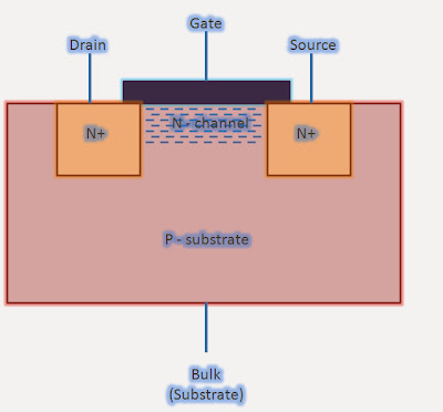
A Metal Oxide Semiconductor Field Effect Transistors (MOSFET, or simply, MOS) is a four terminal device. Figure 1 below shows the general representation of an N-MOS (for PMOS, simply replace N regions with P and vice-versa). MOS is a Voltage-controlled current source as the current through MOS is a function of relative voltage levels of its terminals. The relative voltages of gate, drain and source terminals (assuming bulk or substrate to be at same voltage as source) determine the magnitude of current flowing in MOS. In each of these regions, we can represent the current as a function of gate-to-source voltage (VGS) and drain-to-source voltage (VDS).


A MOS transistor can be considered as a 4-terminal device consisting of source, gate, drain and bulk (substrate).
MOS transistor - a 4-transistor device


In a MOS device, the current flows on formation of channel of carriers between source and drain terminals. For this, voltage at gate terminal needs to be such that it attracts carriers of appropriate type towards itself. When sufficient carriers are attracted towards gate, channel is said to be formed. A current, then, flows between source and drain terminals depending upon the voltage levels of these terminals. The voltage level of substrate also impacts the magnitude of current as it also determines the level of carriers in the channel.

For an N-MOS device, the channel is formed by electrons. So, to attract electrons, gate voltage must be greater than source voltage. For the formation of channel, the difference between VG and VS (VG – VS) must be greater than Vth (threshold voltage of the MOS).

Threshold voltage is defined as the minimum difference in gate-to-source voltage needed for the formation of channel in a MOS device. For NMOS, Vth is positive as for channel formation gate needs to be at higher voltage as explained above. Similarly, for PMOS, Vth is negative as gate needs to be at lower voltage than source for channel to be formed.

On increasing gate voltage beyond threshold voltage, current through MOS increases with increasing gate voltage. Also, if we increase drain voltage keeping gate voltage constant, current increases till a particular drain voltage. After that, increasing drain voltage does not affect the current. Depending upon the relative voltages of its terminals, MOS is said to operate in either of the cut-off, linear or saturation region.

  • Cut off region – A MOS device is said to be operating when the gate-to-source voltage is less than Vth. Thus, for MOS to be in cut-off region, the necessary condition is –
0 < VGS < Vth                           -                       for NMOS
0 > VGS > Vth                                    -                           for PMOS (as threshold voltage of PMOS is negative)

Cut-off region is also known as sub-threshold region. In this region, the dependence of current on gate voltage is exponential. The magnitude of current flowing through MOS in cut-off region is negligible as the channel is not present. The conduction happening in this region is known as sub-threshold conduction.
  • Linear or non saturation region – For an NMOS, as gate voltage increases beyond threshold voltage, channel is formed between source and drain terminals. Now, if there is voltage difference between source and drain, current will flow. The magnitude of current increases linearly with increasing drain voltage till a particular drain voltage determined by the following relations –
VGS ≥ Vth
VDS < VGS – Vth

The current is, then, represented as a linear function of gate-to-source and drain-to-source voltages. That is why, MOS is said to be operating in linear region. The linear region voltage-current relation is given as follows:
Id(Linear) = µ Cox W/L (Vgs – Vth – Vds/2) Vds.
            
Similarly, for P-MOS transistor, condition for P-MOS to be in linear region is represented as:
                        VGS < Vth                        OR                         VSG > |Vth|
            And      VDS > VGS + Vth                           OR             VSD < VSG - |Vth
  • Saturation Region – For an NMOS, at a particular gate and source voltage, there is a particular level of voltage for drain, beyond which, increasing drain voltage seems to have no effect on current. When a MOS operates in this region, it is said to be in saturation. The condition is given as:
VGS ≥ Vth
VDS > VGS – Vth
            The current, now, is a function only of gate and source voltages:
                        Id(saturation) = µ Cox W/L (Vgs – Vth – Vds/2)2