Metastability


What is metastability: Metastability is a phenomenon of unstable equilibrium in digital electronics in which the sequential element is not able to resolve the state of the input signal; hence, the output goes into unresolved state for an unbounded interval of time. Almost always, this happens when data transitions very close to active edge of the clock, hence, violating setup and hold requirements. Since, data makes transition close to active edge of clock, the flop is not able to capture the data completely. The flop starts to capture the data and output also starts to transition. But, before output has changed its state, the input is cut-off from the output as clock edge has arrived. The output is, then, left hanging between state ‘0’ and state ‘1’. Theoretically, the output may remain in this state for an indefinite period of time. But, given the time to settle down, the output will eventually settle to either its previous state or the new state. Thus, the effect of signal present at input of flop may not travel to the output of the flop partly or completely. In other words, we can say that when a flip-flop enters metastable state, one cannot predict its output voltage level after it exits the metastability state nor when the output will settle to some stable voltage level. The metastability failure is said to have occurred if the output has not resolved itself by the time it must be available for use. Also, since, the output remains in-between ‘0’ and ‘1’, which means both P-MOS and N-MOS are not switched off. Hence, VDD is shorted to GND terminal making it cause a high current to flow through as long as the output is hanging in-between.


Metastability example: Consider a CMOS inverter circuit as shown below. The current vs voltage (we can also say power vs voltage as VDD is constant) characteristics for this circuit are also shown. It can be observed that output current is 0 for both input voltage levels; i.e. ‘0’ and ‘1’. As the voltage level is increased from ‘logic 0’, the current increases. It attains its maximum value at ‘Vin’ somewhere near VDD/2. It again starts decreasing as ‘Vin’ is increased further and again becomes 0 when ‘Vin’ is at ‘logic 1’. Thus, there is a local maxima for power consumption for CMOS inverter. At this point, the device is in unstable equilibrium. As for CMOS inverter, for other CMOS devices too, there lies ‘a local maxima’ at some value of input voltage. We all know that for a flip-flop, the output stage is a combinational gate (mostly an inverter). So, we can say that the output of the flip-flop is prone to metastability provided right input level.
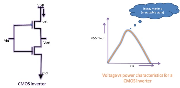

Power characteristics of CMOS inverter
Figure 1: Power characteristics of CMOS inverter

As we now know that a CMOS combinational gate has a point on its ‘voltage characteristic’ curve that is quasi-stable, let us look at a CMOS latch from the same perspective. The CMOS latch has a transmission gate followed by two inverters connected in feedback loop. The voltage characteristic curves for the two inverters are shown. The metastable point, here, lies where the two curves intersect as this point is the resulting peak point of the ‘Superposition curve’ resulting from the two individual curves. A latch goes into metastable state very frequently, especially if the input is changing fast. But, this metastability is resolved quickly as the output tends to go to one of its stable states. As a flop is generally made by connecting two latches in master-slave configuration, the flops are also prone to be metastable. The difference here is just that the probability of a flip-flop being metastable is a lot less than latches as ‘flops are edge sensitive’ as compared to latches which are level sensitive.
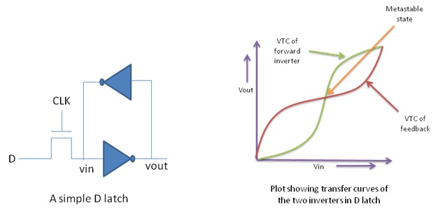

Figure showing transfer curve for D-latch and metastable point
Figure 2: Transfer curves of two inverters in a D-latch


We have just came to know that different elements are prone to metastability to different extents. There is a measure to determine the extent to which an element is prone to metastability failure. This is given by an interval known as ‘Mean Time Between Failures’ (MTBF) and is a measure of how prone an element is to failure. It gives the average time interval between two successive failures. The failure rate is given as the reciprocal of MTBF.
Carry Look Ahead Adder


Carry look ahead adder definition: Carry Look Ahead Adder (CLA Adder) (also known as Carry Look Ahead Generator) is one of the digital circuits used to implement addition of binary numbers. It is an improvement over 'Ripple carry adder' circuit. In Ripple Carry adders, carry propagation time is the major speed limiting factor as it works on the basic mechanism to generate carries as we generally do while adding two numbers using pen and paper. A ripple carry adder may be supposed to be built of a series of 1-bit adders (generally known as a full adder in digital electronics). Thus, the speed of ripple carry adder is a direct function of number of bits. On the other hand, Carry Look Ahead adder solves this problem by calculating carry signals in advance based upon input bits and does not wait for the input signal to propagate through different adder stages. Hence, it implements the adder with reduced delay at the cost of more area (as large combinational logic is required to calculate the look ahead carry as compared to propagated carry).


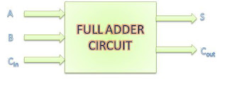
Full adder block diagramShown below is the truth table for a full adder (carry look ahead adder). Ai and Bi are two input bits and Ci is the carry input from the previous stage. Si (Sum) and Ci+1 (Carry out for the next stage) are the outputs for the next stage of the adder. As is evident, carry signal is generated if at least two inputs of full adder are 1 i.e.

  • When both bits Ai and Bi is 1 (regardless of Cin) OR
  • When one of the two inputs (Ai or Bi) is 1 and carry-in (carry of previous stage) is 1


Ai
Bi
Ci
Si
Ci+1
0
0
0
0
0
0
0
1
1
0
0
1
0
1
0
0
1
1
0
1
1
0
0
1
0
1
0
1
0
1
1
1
0
0
1
1
1
1
1
1


The outputs of this full adder, when expressed in the form of a boolean expression can be written as a function of inputs as follows: 
          
        Si = Ai xor Bi xor Ci
        Ci+1 = Ci(Ai xor Bi) + AiBi


Where Si is the sum bit calculated for nth adder stage and Ci+1 is the carry out from nth stage and will act as input for n+1th stage. For an N stage ripple carry adder, there is overhead of calculating the carry out of kth stage before carry out of k+1th stage can be calculated. If we go deeper into analysis, it comes out that ck+1 is a function of c0 and is discussed below. Let the intermediate outputs from a full adder stage be represented as Pi and Gi given as below:

          Pi = Ai xor Bi 
          Gi = Ai.Bi
          Si = Pi xor Ci
          Ci+1 = Ci.Pi + Gi


  •  Gi is known as carry generate signal since carry (Ci+1)is generated whenever Gi= 1 regardless of Ci
  • Pi is known as carry propagate signal since whenever Pi = 1, Ci+1 = Ci (when Pi=1, Gi = 0)
Thus, recursively replacing the values for Ci for each Ck, we can write the boolean expression of carry outputs of various stages in terms of C0 and Pk's as follows:

C1 = C0P0 + G0C2 = C1P1 + G1 = (C0P0+G0)P1 + G1 = C0P0P1 + P1G0 + G1C3 = C2P2 + G2 = (C0P0P1 + P1G0 + G1)P2+G2 = C0P0P1P2 + P2P1G0 + P2G1 +           G2C4 = C3P3 + G3 = (C0P0P1P2 + P2P1G0 + P2G1 + G2)P3 + G3 = C0P0P1P2P3 +             P3P2P1G0 + P3P2G1 + G2P3 + G3
Thus,
         Ci = F(P,G,C0)

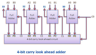
4-bit carry look ahead block diagram
4-bit carry look ahead adder block diagram
In other words, carry signal is a direct SOP (Sum of Products) expression of C0 (usually 0) and input signals rather than its preceding carry signal. Let us illustrate taking a 4-bit adder as an example. This expression can be used to construct a carry look-ahead adder of any number of bits.

A 4 bit Carry Look Ahead (CLA) adder can be constructed with the help of following steps (Assuming T as the delay of a single 2-Input gate):
  1. Generate All P and G internal signals. These can be generated simultaneously as C0 and all inputs are available. 
  2. Generate all carry output signals (C1, C2, C3, C4). These will be valid after 3T time
  3. Generate Sum signals S = P xor C. It will be valid after 4T time.
Thus, Sum signals will be valid after a delay of 4T. On the other hand, delay expression in case of ripple carry adder = (2n+2)T. Thus, for n =4, i.e. for 4 bit ripple carry adder, delay will be 10T.

For higher order addition, boolean expression of carry output becomes more complex. So, there is tradeoff between area and speed. For larger number of bits, increase in area is more than speed advantage obtained. Hence, Carry Look Ahead adders are usually implemented as 4-bit modules that are used to build larger size adders.

Below is a nice video that explains about carry look ahead adders (taken from youtube).