MBIST (Memory Built-In Self Test)


The ever increasing size and number of memories in the Systems on Chip has presented the designers and test engineers with a challenge for huge number of functional or ATPG patterns for verification of memory functionality. So, to test the memory functionality either functionally or through ATPG requires huge test time, and hence, huge test cost. It is almost impossible in such scenario to verify memory functionality fully. Thus, the designers are left with only one way; i.e. to verify memory functionality through BIST (Built-In Self Test) functionality.


BIST is an inbuilt testing circuitry within a software/hardware module. We just need to trigger the circuitry from outside. This circuitry, then, runs the inbuilt patterns/algorithms and returns if the module is working properly. This, being inbuilt does not need to be supplied with patterns from outside. Also, since, this is within a module, hence, we can take the modular approach for testing which reduces run time significantly.


Figure to show mbist interface. MBIST testing involves a mbist controller+pattern generator that controls the testingThe built-in self test employed for memories is known as MBIST (Memory Built-In Self Test). Like other BIST logic, MBIST logic is inbuilt within memory only. The MBIST logic may be capable of running several algorithms to verify memory functionality and test for memory faults specifically designed and optimized for these.


There is usually a wrapper around memory, known as ‘memory collar’ that is used to select between functional inputs and test inputs based upon MBIST/functional mode selection bit. It interfaces the memory with on-chip logic and MBIST controller. The MBIST controller indicates the start of MBIST with a select input. The memory, then, starts the BIST algorithms and provides the test output to the controller. The controller compares this output with the reference output and indicates if the MBIST has passed or failed. There can be one controller for several memories. Also, memories can share the collar depending upon the test time requirement and type of memories.


Advantages of MBIST: There are several advantages of MBIST insertion over functional/atspeed testing such as:

  • It allows for robust testing of memories 
  •  Reduced test time 
  •  All the memories of the design can be tested in parallel 
  •  Lesser test cost


Disadvantages of MBIST: Inspite of many advantage of MBIST, there is only one remarkable limitation. Insertion of MBIST causes increase in area. However, this increase in area is very small in comparison to the benefits it provides.

Related posts:
Latchup and its prevention in CMOS devices

What is Latchup: Latchup refers to short circuit formed between power and ground rails in an IC leading to high current and damage to the IC. Speaking about CMOS transistors, latch up is the phenomenon of low impedance path between power rail and ground rail due to interaction between parasitic pnp and npn transistors. The structure formed by these resembles a Silicon Controlled rectifier (SCR, usually known as a thyristor, a PNPN device used in power electronics). These form a +ve feedback loop, short circuit the power rail and ground rail, which eventually causes excessive current, and can even permanently damage the device.
      
                                                                 
Latchup refers to short circuit formed between power rails in an IC leading to high current and damage to the IC. Speaking about CMOS transistors, latch up is the phenomenon of low impedance path in CMOS between power rail and ground rail due to interaction between parasitic pnp and npn transistors. The structure formed by these resembles a Silicon Controlled transistor (SCR, usually known as a thyristor, a PNPN device used in power electronics). These form a +ve feedback loop, short circuit the power rail and ground rail, which eventually causes excessive current and even permanently damage the device.
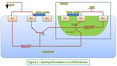
Figure 1: Latchup formation in CMOS
Latchup formation: Shown alongside is a CMOS transistor consisting of an NMOS and a PMOS device. Q1 and Q2 are parasitic transistor elements residing inside it. Q1 is double emitter pnp transistor whose base is formed by n well substrate of PMOS, two emitters are formed by source and drain terminal of PMOS and collector is formed by substrate(p type) of NMOS. The reverse is true for Q2. The two parasitic transistors form a positive feedback loop and is equivalent to an SCR (as stated earlier).

Analysis of latchup formation: Unless SCR is triggered by an external disturbance, the collector current of both transistors consists of reverse leakage current. But if collector current of one of BJT is temporarily increased by disturbance, resulting positive feedback loop causes current perturbation to be multiplied by β1β2 as explained below. The disturbance may be a spike of input voltage on an input or output pin, leading to junction breakdown, or ionizing radiations.

Because collector current of one transistor Q1 is fed as input base current to another transistor Q2, collector current  of Q2, Ic2 =  β2 * Ib2 and this collector current Ic2 is fed as input base current Ib1  to another transistor  Q1. In this way both transistors feedback each other and the collector current of each goes on multiplying.

Net gain of SCR device = β1 *β2

Total current in one loop = current perturbation * Gain

If     β1 *β2 >=1, both transistors will conduct a high saturation current even after the triggering perturbation is no longer available. This current will eventually becomes so large that it may damage the device.

Latch-up prevention techniques: Simply put, latchup prevention/protection includes putting a high resistance in the path so as to limit the current through supply and make β1 *β2 < 1. This can be done with the help of following techniques:

  • Surrounding PMOS and NMOS transistors with an insulating oxide layer (trench). This breaks parasitic SCR structure.
  • Latchup Protection Technology circuitry which shuts off the device when latchup is detected.

Read NextRegions of operation of MOS transistors