Design problem: A set of flip-flops, some working on 100 MHz clock and others working on 200 MHz clock are required to come out of reset together. What should be the clock of reset synchronizer
Solution: Since all the flip-flops are required to come out of reset in the same cycle, all these must get reset from a single reset synchronizer. Now, as the question states that the flip-flops in the fanout of reset synchronizer are working on two clocks. We need to find the correct-by-design clock that reset synchronizer should be working on. Let us assume that the correct clock to be connected to reset synchronizer is one of the two frequencies given.
 |
| Figure 1: Reset synchronizer |
First, let us check by assuming that reset synchronizer works on positive edge of 100 MHz clock. Figure 2 shows the setup checks for 100 MHz -> 100 MHz and 100 MHz -> 200 MHz paths. Let us say, reset deassertion propagates to R1/Q at edge (1). Going by figure 2, all flip-flops working on 200 MHz clock will be out of reset at edge (3) and all flop-flops working on 100 MHz will be out of reset at edge (5). Thus, reset synchronizer working on positive edge of 100 MHz clock does not solve our purpose.
 |
| Figure 2: Reset synchronizer works on positive edge of 100 MHz clock |
Now, let us check the same when reset synchronizer works on positive edge of 200 MHz clock. In this case, reset can deassert either on edge (1) or edge (3). If reset deasserts on edge 3, then, we have both the categories of flops coming out of reset at same time edge (5). But if reset deasserts on edge (1), both categories of flops get out of reset at different times. Thus, we can get the reset synchronizer working on 200 MHz clock, but we have to ensure by design that reset gets deasserted on the edge of 200 MHz clock that coincides with negative edge of 100 MHz clock. Figure 3 and figure 4 discuss these scenarios.
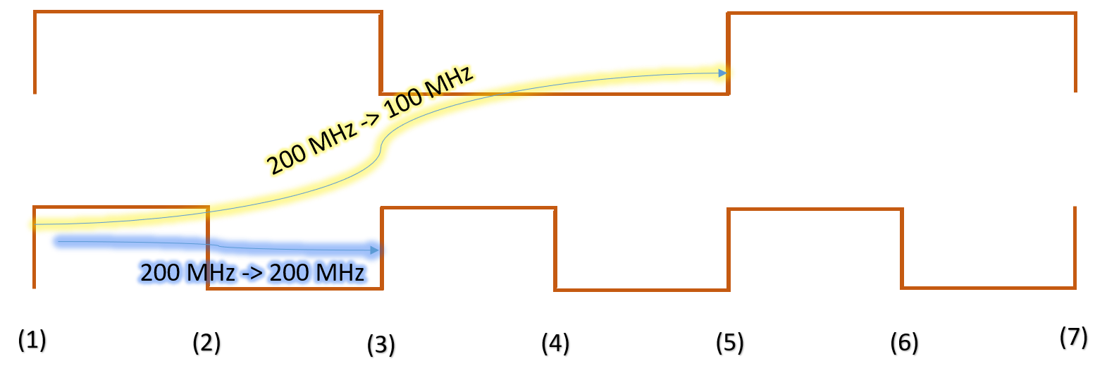 |
| Figure 3: Reset synchronizer works on positive edge of 200 MHz clock coinciding with positive edge of 100 MHz clock |
 |
| Figure 4: Reset synchronizer works on positive edge of 200 MHz clock coinciding with negative edge of 100 MHz clock |
Now, let us explore the last option; i.e., reset synchronizer working on negative edge of 100 MHz clock. In this case, as shown in figure 5, both 100 MHz and 200 MHz flip-flops come out of reset on same edge. Thus, this case works perfectly. Figure 5 illustrates this.
 |
| Figure 5: Reset synchronizer works on negative edge of 100 MHz clock |
Can you provide any other solution that is possible and better than ones discussed here.
