Design problem: Clock gating for a shift register

Problem: There is an 4-bit shift register with parallel read and write capability as shown in the diagram. We need to find out an opportunity to clock gate the module.

 Mode selection bits ("S1" and "S0") are controlling the operation of this shift register with following settings:

Solution: From the basics of clock gating, we know that if the stae of a flip-flop is not chaging, there lies an opportunity to gate its clock. Observing the table, we see that state of all flip-flops does not change when "S1,S0" are either "00" or "11". So, when mode selection bits are corresponding to these values, we can gate the clock to this shift register. Or, we can say that clock to the module should reach only when (S1 xor S0) is equal to 1.


Can you relate the timing of S1 and S0? Should they be coming from positive edge-triggered flip-flop or negative edge-triggered flip-flop? Clock gating checks explains the timing of clock gating signals with respect to clock.

Also read:


MOS transistor structure

A MOSFET (Metal Oxide Semiconductor Field Effect Transistor), or MOS, as is commonly called, is an electronic device which converts change in input voltage into a change in output current. The basic structure of a MOS transistor (as seen sideways) is as shown in figure 1. The substrate is a lightly doped semiconductor. Source and Drain regions are heavily doped regions of type opposite to substrate. In-between source and drain is a region called channel. Above the channel is a very thin layer of oxide. 

The voltage is applied to input terminal, which is called "Gate" terminal. If sufficient voltage is applied at the gate terminal, a channel gets formed between source and drain terminals. Depending upon the nature of channel formed, MOS is termed as N-MOS or P-MOS.

N-MOS: For an N-MOS, substrate is P-type, source and drain regions are N-type. Application of a positive voltage at Gate terminal with respect to substrate will result in formation of channel of electrons.

P-MOS: For a P-MOS, substrate is N-type, source and drain regions are P-type. Application of a negative voltage at Gate terminal with respect to substrate will result in formation of channel of holes.


What is the difference between a normal buffer and clock buffer?

A buffer is an element which produces an output signal, which is of the same value as the input signal. We can also refer a buffer as a repeater which repeats the signal it is receiving, just as there are repeaters in telephone signal transmission lines. You must have noticed that we have two kinds of buffers (or any logic gate) available in standard cell libraries as:

  • Clock buffer: The clock buffers are designed specifically to have specific properties that are supposed to be good for clock distribution networks (clock trees). The specific properties that are required in an ideal clock tree buffer are given as below. However, it is not possible to attain these ideal properties for every buffer at every technology node. It may be only possible to get close to these properties.
    • Equal rise and fall times
    • Less delays
    • Less delay variations with PVT and OCV
  • Normal buffer/data buffer: For a data buffer, the above properties are usually less desired
Usually, we can say that following differences may exist between a clock buffer and a normal buffer:
  • In SoCs, clock routing is done in higher metal layers as compared to signal routing. So, to provide easier access to clock pins from these layers, clock buffers may have pins in higher metal layers. That is, vias are provided in standard cell itself instead of necessitating on having in clock distribution network. For a data buffer, the pins are expected to be in lower layers only.
  • Clock buffers are balanced. In other words, rise and fall times of clock buffers are nearly equal. The reason behind this is that if the clock buffers are not balanced, there will be duty cycle distortion in the clock tree, which can lead to pulse width violations as discussed in minimum pulse width violation example. On the other hand, data buffers can compromise with either of rise/fall times. In other words, they dont need to have PMOS/NMOS size to be 2:1; and hence, can be of smaller size as compared to clock buffers.
  • Due to above reason, clock buffers consume more power as compared to normal buffers.
  • Generally, you will find clock buffers with higher drive strength as compared to normal buffers. So that a clock buffer can drive long nets and can have higher fanouts. This helps clock buffers, and hence, clock trees to have less overall delays.

Performance gain with latches

The property of latches being transparent gives them a basic characteristic, known as time borrowing, owing to which they can capture data over a period of time rather than an instant. Using this property of latches intelligently can result in performance advantage for specific design scenarios, especially for designs having asymmetric data paths in subsequent stages. Let us elaborate with the help of an example.
Let us suppose a design having two stages of pipeline with combinational logic in each stage as 12 ns and 5 ns respectively as shown in figure 1 below:

Figure 1: 2-stage pipelining

If we assume clock period to be 16 ns (half cycle being 8 ns), then each latch stage will borrow time from the subsequent stage as shown in figure below:


.

Now, since all the registers get the same clock signal, the minimu clock period is the maximum of combinational delays from REGA to REGB and REGB to REGC.

Tclk > MAX (TcombregA->regB, Tcombr(regB->regC))


Thus, this circuit cannot run with half clock period less than 12 ns, or clock period less than 24 ns.

This situation can be easened up if we replace REGB with a negative level-sensitive latch. Let us have a look at figure 2 below. Although the number of stages still remains the same, LATB can borrow time from next stage without impacting any logic.

Figure 2: Latch replacing register in the 2-stage pipelining
The same is shown in figure 3 below with the help of waveform. The clock is having a period of 9 ns. The latch can borrow time of 3 ns from next stage, still meeting the setup time by 1 ns. Thus, we have succeeded in reducing the half time period from 12 ns to 9 ns (time period from 24 ns to 18 ns), just by changing the register to a latch. This is how a latch can help gain in performance.

If there are multiple latch stages in series, each can borrow from the subsequent stage such that overall timing is met. For example, figure 3 shows 6 latches in series.


How delay of a standard cell changes with drive strength

A standard cell (let us say a buffer) can be represented as shown in figure 1 below, where 
R = Channel resistance 
Cds = Drain-to-source capacitance (internal capacitance of cell)
Cload = Load capacitance


So, RC time constant can be represented as "R * (Cds + Cload)".

What happens on increasing the drive strength? In our post "what is meant by drive strength", we discussed that the drive strength of a standard cell increases when we increase the size of its transistors. So, basically, a cell with drive strength 2X will have twice of width as compared to the one with 1X drive strength.
And we know that
Channel resistance decreases with "W".
Drain-to-source capacitance increases with "W".
So,  upon increasing the drive strength, its internal capacitance will increase and channel resistance will reduce by same amount. The same is depicted in figure 2 below.


Time constant of "1X" buffer = R * (Cds + Cload)
 Time constant of "2X" buffer = R/2 * (2Cds + Cload) 
Now, let us talk of following scenarios:

Special case 1: Load capacitance is negligible.
In this scenario, we are left with only internal resistance and capacitance of the cell.

Time constant of "1X" buffer = R * Cds
Time constant of "2X" buffer = R * Cds
So, in this case, there should not be any impact of increasing the drive strength of standard cell on delay. So, in case there is negligible load, we should not upsize the standard cell. Doing so may instead increase the overall path delay as increased drive strength cell will present increased load to the previous stage cell, thereby increasing the delay of previous stage.

Special case 2: Load capacitance is very large as compared to internal capacitance.
In this scenario,
Time constant of "1X" buffer = R * Cload
Time constant of "2X" buffer = (R * Cload ) / 2 
So, second buffer will take approximately half the time to charge the load capacitance as compared to "1X" buffer.

So, we see that the the maximum possible benefit in delay by increasing the drive strength of standard cell is a reduction by a factor of two. In the worst case, we may not see any benefit at all.

We can also look at above equation by splitting cell delay into two components:
  1. Cell delay due to its own intrinsic capacitance: It does not scale by drive strength and is a constant value for one kind of standard cells.
  2. Cell delay due to external load capacitance: It is variable and decreases as we increase the drive strength of standard cell.

What is meant by drive strength of a standard cell

As we know that cell delay is a function of output load capacitance. The most simplistic equivalent circuit of a logic gate driving an output can be assumed as given in figure 1:


The purpose of logic gate is to propagate the effect of logic value available at its input to the output. Based upon whether '0' or '1' is to be propagated to the output. The corresponding is achieved by charging and discharging of the output load capacitance. Propagating a logic '0' will mean discharging of the load capacitance, and vice-versa. Drive strength of the logic gate is the its relative capability to charge/discharge the capacitance present at its output. Now, the time constant, and hence, delay of the circuit is "RC".
So, for a cell with higher drive strength, corresponding "R" is lesser than the one with lower drive strength. So that for same load capacitance "C", delay is lower for a cell with higher drive strength as it can charge the capacitance in lesser time.

How drive strength varies with size of a cell: Let us talk in terms of MOSFETs, although this is valid in terms of every device in general. We know that for a given technology standard cell library, length of all transistors is kept constant. For instance, 90 nm technology will have gate length of all transistors as ~90 nm. And channel resistance of the MOSFET is inversely proportional to "W/L" of the transistor. So, a simple way to decrease channel resistance is to increase "W" of the transistor. So, a transistor with more area will have lesser resistance. Or we can say that a logic gate with bigger transistors will have more drive strength.

What is unit drive strength: In a standard cell library, we generally see cells labelled as "1X", "2X" and so on. But what is meant by the number that you see with drive strength? In general, the lowest size logic gate is labelled as unit drive strength. The drive strength numbers of other cells are laelled relative to unit drive strength cell.

Read next: How delay of a cell changes with drive strength

Also read:

Why setup is checked on next edge and hold on same edge? Setup and hold – the state machines essentials

Hi friends, in the post State machines – a practical perspective, we learnt about state machines. We also discussed different aspects of a state machine with the help of an example and the need of setup and hold checks to be taken care of. In this post, we will be discussing the state machine with a pinch of setup and hold and try to build a better understanding regarding these. For recapitalization, see figure 1. Each clock edge in a digital state machine represents a state. At each clock edge, all the registers in the design update their value based upon the data available at their input which is based upon the value computed on the basis of values launched by some other registers at previous clock edge. In simplest of words, state 3 is dependent upon state 2, which, in turn, is dependent upon state 1 and so on.

Each state of a state machine can be represented by a clock pulse
Figure 1: State machine representation of a clock pulse

All digital systems are synchronous systems (state machines) that require all the elements of the state machine to be in harmony. For instance, let us say, a state machine has 100 registers. All these registers need to be updated at the same time and need synchronized inputs so as to have only valid states in the state machines. For digital synchronous state machines, all the registers are synchronized by a clock signal. This is ensured with the help of setup and hold checks. But why do we need to apply setup and hold checks, is the question still unanswered.

Why setup and hold? We often encounter people saying that meeting the setup and hold requirements of a design is critical for silicon functionality. But have you ever thought why it is so? As we now know from our previous post, for a design consisting of only positive edge-triggered registers, each positive clock edge corresponds to a state and the state of the machine is updated at every clock edge since all the flip-flops capture data. In other words, the state of the machine is a function of the values of the registers at a particular clock cycle. For proper state machine functioning, the values launched from one register at one clock edge should be available at the input of the capturing flop before next clock edge arrives and should be available only after the present clock edge has passed (will become clear later on). This is necessary in order that the next state of the state machine is a valid state. If this does not happen, the state of the machine will not be what is desired. It may also happen that the state machine goes altogether into an invalid state leading to undesired results. And this is the reason setup is checked on the next edge and hold on same edge as discussed below.
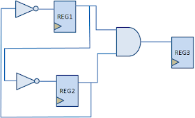
Let us assume a hypothetical state machine consisting of three registers and some logic gates as shown in figure 2 below. If we assume the initial outputs of REG1 and REG2 to be 1 and 0 respectively, then the possible states can only be 100 or 010.

The shown state machine consists of three registers
Figure 2: A state machine with three registers and some logic

The state transition table for this state machine is as shown in figure 2. As is shown, there are only two valid states (100 and 010) provided the initial state of REG1 and REG2 is different (10 or 01). The state of REG3 is supposed to remain always ‘0’ as the REG1 and REG2 are supposed to always have different values at a time (given initial condition is also this).
State diagram of state machine shown in figure 2
Figure 3: State diagram of state machine shown in figure 2

The states with respect to clock waveform are as shown in figure 4 below. As is expected, each clock edge corresponds to one of the two states.

Figure 4: Clock waveforms showing different states of state machine

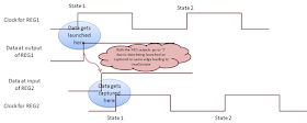
Now, the state of register 2 at a particular state (clock edge) depends upon state of register 1 at the previous clock edge. Let us assume register 2 is getting delayed clock with respect to register 1. In other words, there is considerable positive skew between the two registers. In this case, as shown in figure 5 below, there is a good chance that the data launched from register 1 is captured at register 2 at the same edge and not the next clock edge. Due to this, both register 1 and 2 will have same value at a particular clock cycle and the machine will run into invalid state. The data getting captured at the same edge as the launch flop is termed as hold violation (unless it is architecturally intended, the discussion of this is outside the scope of this topic).
The hold violation results due to data being captured on the same edge as it is launched on
Figure 5: Hold violation resulting in state machine going to invalid state
Similarly, for the proper functioning of the state machine, the data launched at one edge should get captured at the next edge. This is what is termed as setup check. Thus, setup check is formed on next edge only. The failure in happening so is termed as a setup violation. Similarly, the data launched at one edge should not be captured on the same edge. Thus, hold check represents this situation and ensures that the data launched on one edge is not captured on the same edge.

Based upon development of our understanding in this post, setup and hold can be defined as:

Setup check: Setup check refers to the condition in which data launched at one clock edge should get captured at the next clock edge so that the state machine functionality is preserved and the state machine transitions smoothly from one state to the next. The failure in happening so is termed as setup violation and the state machine might transition to an invalid state.


Hold check: Hold check refers to the condition in which data launched at one clock edge should not get captured at the same clock edge so that present state of the state machine does not get corrupt. The failure in happening so is termed as hold violation and the state machine might transition to an invalid state.

Design problem: How can you convert an XOR gate into a buffer or an inverter?


Figure 1 above shows the truth table of a 2-input XOR gate. It has two inputs A, B and an output OUT. On looking closely, we observe that:

  • If one of the inputs (say B) is 0, OUT is equal to the other input. For instance, when B = 0,
    • OUT = 0 when A = 0
    • OUT = 1 when A = 1
  • Similarly, if one of the inputs is 1, OUT is equal to invert of the other input. For instance, when B = 1,
    • OUT = 1 when A = 0
    • OUT = 0 when A = 1
Using the above information, XOR gate can be easily converted to a buffer and an inverter.

Buffer using XOR gate: Simply connecting one of the inputs to logic '0' will convert XOR gate into a buffer. As shown in the truth table below, OUT is following the value of B.


Inverter design using XOR gate: Similarly, we can realize an inverter using an XOR gate by connecting one of the inputs to logic '1'. As shown in the truth table below, OUT is opposite to the value of B.


Minimum pulse width violation example

STA problem: Consider below figure, wherein minimum pulse width requirement of a flip-flop is 590 ps. It is getting clocked by a PLL of 500 MHz with a duty cycle variation of 60 ps. There are 30 buffers in clock path, each having a rise delay of 60 ps and fall delay of 48 ps. Will this setup be able to meet the duty cycle requirement of flip-flop? Find the slack available.


Solution:

Here, we must remember that pulse can be either high pulse or low pulse. So, we need to check for both. Let us start with high pulse:

Pulse width check for high pulse: Here, we are left with calculating the latest possible arrival of rising edge and earliest possible arrival of falling edge at the flip-flop. It is given that

Ideal clock period = 2000 ps (500 MHz frequency)
Ideal half cycle = 1000 ps
Duty cycle variation of clock source = 60 ps
So, if we assume that positive edge of the clock has arrived at 0 time, negative edge can arrive at any time between 940 ps (1000 - 60) and 1060 ps (1000 + 60). Taking the pessimistic case, we have to assume negative edge arrives at 940 ps thereby making the high pulse as 940 ps at clock source.

Now, there are 30 buffers with rise delay of 60 ps and fall delay of 48 ps.

Rising edge will reach flip-flop at time (0 + 30 * 60) = 1800 ps.
Falling edge will reach flip-flop at time (940 + 30 * 48) = 2380 ps
Effective pulse width visible at flip-flop = 2380 - 1800 = 580 ps

Now, the pulse width requirement = 590 ps
Slack = Actual pulse width = Required minimum pulse width = -10 ps

So, we are violating the minimum high pulse width requirement by 10 ps.

Pulse width requirement for low pulse: Similar to the earlier case, we have to find the difference in arrival of latest negative edge and earliest positive edge.

Ideal clock period = 2000 ps (500 MHz)
Ideal half cycle = 1000 ps
Duty cycle variation of clock source = 60 ps
If we assume that negative edge arrived at 0 ps, positive edge can arrive at any time between 940 ps and 1060 ps. Taking the pessimistic case, low pulse width = 940 ps at clock source.

Now, there are 30 buffers with rise delay of 60 ps and fall delay of 48 ps.

Falling edge will reach flip-flop at time (0 + 30 * 48) = 1440 ps
Rising edge will reach flip-flop at time (940 + 60 * 30) = 2740 ps
Effective pulse width visible at flip-flop = 2740 - 1440 = 1300 ps

Pulse width requirement = 590 ps
Slack = 1300 - 590 = 710 ps

So, we are meeting the low pulse width requirement by 710 ps.

Glitches in combinational circuits

What is a glitch: As per definition, a glitch is any unwanted pulse at the output of a combinational gate. In other words, a glitch is a small spike that happens at the output of a gate. A glitch happens generally, if the delays to the combinational gate output are not balanced. For instance, consider an AND gate with one of its inputs getting inverted and delayed version of  its other input. It, then will produce a short pulse (or glitch) at the ouput whenever its input goes from zero to one.


As also said above, this is due to the fact that the delays to the AND gate through two paths are not balanced. Let us elaborate with the help of below waveform. When input goes from zero to one, the other input will go to zero after some time as there is a delay equal to that of an inverter. Due to this, there will be a glitch at the output of AND gate. It needs to be noted that lesser the delay difference between the two inputs at the input of AND gate, lower will be the duration of glitch.


How are glitches harmful? Glitches may be harmful in two ways:

  • Timing/functional issue: A glitch can be an issue if it propagates to the resultant logic or gets captured by a flip-flop. There can be two cases here:
    • Synchronous timing paths: These are timing paths wherein we are required to meet setup and hold timings. So, even if there is a glitch, it will be within the limits of minimum and maximum delays permissible from one flip-flop to another. So, there will be no timing issue provided that you have taken care of setup and hold timings.
    • Asynchronous timing paths: If the launch and capture clocks do not have any relationship, setup and hold cannot be ensured. So, if there is a glitch in the data path, it can get captured, hence, can cause issue. To prevent this, synchronizers are used and there are certain rules to be followed for asynchronous paths. These are to be followed to ensure that no wrong data gets captured due to clock glitches. It should be better to call this as functional issue as it can be taken care of only architecturally.
  • High power!!! Every toggling causes power dissipation due to charging and discharging of gate capacitance. So, a glitch causes power dissipation. Even if there is no timing/functional issue associated with the glitch propagation, power dissipation can be an issue. Larger the combinational path leading to a node, larger the number of probable toggles possible; greater is the expected power dissipation.

Help improve this post!! - mail us the suggestion at myblogvlsiuniverse@gmail.com

How to fix min pulse width violation

In our previous posts, we discussed about the duty cycle, duty cycle variation and duty cycle degradation. Bad duty cycle impacts half cycle timing paths and has impact in meeting timing for minimum pulse width checks of flip-flops. However, there are certain techniques available that can help you in improving the duty cycle of the clock. We will discuss these techniques in this post as below:

1. Dual inversion in clock branch: A certain category of logic cells are more probable of having one of the rise or fall delays greater than the other. A chain of such cells will make either high pulse of clock shorter or low pulse of clock shorter. One can use an inverter in the middle of the chain as shown in figure below to tackle this. Doing this, what we are essentially doing is converting rise edges to fall and vice-versa. So, the shortening of pulse of first few elements is balanced with the rest of the elements. In the below figure, there are 20 buffers, each shortening the pulse by 10 ps. The output of 10th buffer will have a shorter pulse as compared to clock source. The inverter at the output of 10th buffer will feed an inverted clock to 11th buffer. This will have high pulse which is greater than low pulse. Rest of the chain will try to reduce this pulse. In the end, we get a pulse which is equal to what was available at the source.


One can also try an all-inverter clock tree. In an all-inverter clock tree, every element will change the sense of clock pulse; thereby minimizing the clock pulse distortion.

However, this kind of delay balancing will only work where there is inherent variation of delays in rise vs fall. It will not work in case of OCV variations. So, if the chain length is arbitrarily large, our second method will come to rescue.

2. Even division to tackle duty cycle degradation: Suppose there is source clock with very poor duty cycle (say 10%) and you divide down the clock by 2 with a flip-flop divider. What we observe is amazing. The resulting clock is having almost 50% duty cycle. So, whenever we need an output clock with perfect duty cycle, we can use a divider to divide down the clock. The only drawback of this method is that we need a source clock of frequency twice than what is required to be timed!!


There are a few things to be kept in mind for this method:

  • This method will improve the duty cycle of clock at the output of the flop. Degradation in duty cycle happening after the divider, if any, will be there.
  • Duty cycle of the input clock at flip-flop must be within the limits of what is required to be minimum pulse width at the flip-flop.

Duty cycle degradation

In the post, we discussed about duty cycle variation of the clock source. However, this is not the only pain in half cycle timing paths. Along clock path also, duty cycle of the clock can degrade. This can effect timing of half cycle paths adversely. We will discuss this in some detail; and also discuss how to tackle this. 

How is there degradation in duty cycle of clock: In addition to source duty cycle variation, there can be assymmetry in rise delay vs fall delay of clock elements. For instance, a buffer may have nominal rise (0 -> 1) delay of 50 ns whereas 48 ns for fall delay (1 -> 0). So, if a clock pulse passes through it, it will eat a portion of this clock pulse as shown in figure 1 below. For more clarity, we have exaggerated the scenario with a fall delay of 30 ns.


There are a lot of delay elements in clock distribution networks (also called clock tree network) inside the SoC. So, this problem is bound to happen there. Let us say, clock path has 20 buffers, each having a rise delay 10 ps greater than fall delay. So, the high pulse will get shortened when the clock reaches its sink. See how the pulse gets shortened if there is asymmetry in rise vs fall delay of a delay element or logic gate in below figure.


Even if we assume that the delay element has rise delay equal to fall delay, still, there is possibility of duty cycle degradation. Normally, a buffer (or inverter) has a nominal delay with some delay variations (for instance, OCVs) to be taken into account. For instance, it may have a rise delay of 100 ps with OCV variation to be taken of 5%. So, depending upon the scenario, we need to take its delay as either 95 ps or 105 ps. Similarly, even if we say that fall delay is exactly equal to rise delay, even then because of OCV variations, fall delay to be taken into account will be different than rise delay. Let us suppose, there are 20 such buffers in clock path with an ideal clock source. Then, we will have uncertainty in arrival of both rise and fall edges. And the effect will be visible in timing paths' slack.


How duty cycle degradation impacts timing: Degradation in duty cycle impacts timing wherever both rising and falling edges of clock are involved. For instance, it will impact half cycle timing paths as well as minimum pulse width check. You can go through our post duty cycle of clock to have an idea of the impact.


Duty cycle variation of inter-clock timing paths

In the post, duty cycle variation, we understood what duty cycle variation is, and how to apply for intra-clock timing paths. But of similar importance is duty cycle variation as applied to inter-clock timing paths. Let us discuss these cases one-by-one:

Root clock to root-inverted clock: Inverted clock is same as root clock in frequency, with phase inverted. So, duty cycle variation needs to be applied for following cases:

  • Root rise edge -> generated rise edge
  • Root fall edge -> generated fall edge
  • Generated rise edge -> Root rise edge
  • Generated fall edge -> Root fall edge

Following commands will be needed to be applied:
set_clock_uncertainty -rise_from root_clk -rise_to gen_clk <duty_cycle> 
set_clock_uncertainty -fall_from root_clk -fall_to gen_clk <duty_cycle>
set_clock_uncertainty -rise_from gen_clk -rise_to root_clk <duty_cycle>
set_clock_uncertainty -fall_from gen_clk -fall_to root_clk <duty_cycle>

Root clock to odd 50% divided clock: In this scenario, we need to apply extra uncertainty for the following cases:

  • Root rise edge -> Generated fall edge
  • Root fall edge -> Generated rise edge
  • Generated rise edge -> Root fall edge
  • Generated fall edge -> Root rise edge


Following commands will need to be applied for this case:
set_clock_uncertainty -rise_from root_clk -fall_to gen_clk <duty cycle>
set_clock_uncertainty -fall_from root_clk -rise_to gen_clk <duty cycle>
set_clock_uncertainty -rise_from gen_clk -fall_to root_clk <duty cycle>
set_clock_uncertainty -fall_from gen_clk -rise_to root_clk <duty cycle>

Root clock to even 50% divided clock: In this case, we need to apply duty cycle uncertainty for the following cases:

  • Root fall edge -> Generated rise edge
  • Root fall edge -> Generated fall edge
  • Generated rise edge -> Root fall edge
  • Generated fall edge -> Root fall edge
Below figure shows these cases for a 50% divided clock from root clock.


So, the rule of thumb is same. Wherever there is a timing path wherein both rising and falling edges of root clock are involved, duty cycle variation will come into play. If you just keep this basic thing into mind, duty cycle variation will never haunt you. :-)

Also read:

Duty cycle variation

Duty cycle variation: Similar to jitter in clock period, there can be variations in duty cycle of the clock source due to uncertainty in the relative timings of positive and negative edges. Duty cycle variation is always measured with respect to corresponding positive and negative edges. In other words, we can also say that duty cycle variation is the uncertainty in arrival of negative edge, given that positive edge has arrived at certain fixed point of time. Let us take an example. If we are given a clock with a period of 10 ns with ideal 50% duty cycle. Also, we are given that it has the clock has a duty cycle variation of +-5%. So, if we say that we saw positive edge of clock at 100 ns, we can expect to see negative edge of clock at any time between 14.5 ns and 15.5 ns. The timing waveform in figure 2 illustrates this. 


Similarly, if we know with certainty, the point of arrival of negative edge, there will be uncertainty in the time of arrival of positive edge of the clock.

Applying duty cycle variation: There may be specific command in STA tools to specify duty cycle variation of a clock. If that is available, you just need to specify duty cycle variation of the master clock source. And all the above discussed cases will be taken care automatically by the tool. If not, it can be applied with the help of SDC command "set_clock_uncertainty". For instance, to apply duty cycle variation for a clock named "clk" of 0.5 ns, we can apply following commands:
set_clock_uncertainty -rise_from clk -fall_to clk 0.5 -setup
set_clock_uncertainty -fall_from clk -rise_to clk 0.5 -setup
set_clock_uncertainty -rise_from clk -fall_to clk 0.5 -hold
set_clock_uncertainty -fall_from clk -rise_to clk 0.5 -hold 

Note that there are two commands that need to be applied as there are two categories of half cycle paths, rise-fall and fall-rise. 

Timing implication of duty cycle variation: The same way as clock period jitter impacts setup slack of full cycle timing paths; duty cycle variation plays a role in half cycle timing paths. That is why, duty cycle variation is also referred as half cycle jitter. Keeping in mind that there are a lot of cases available with divided and undivided clocks, we will discuss below how to apply duty cycle variation while calculating timing slack. We need to keep in mind that, simlar to full cycle jitter, duty cycle variation is the property of a clock source. With reference to duty cycle variation, there can be following categories of clocks.

  • Master clock
  • Even divided clocks from master clock with 50% duty cycle
  • Odd divided clocks from master clock with 50% duty cycle
  • Even divided clocks from inverted master clock with 50% duty cycle
  • Odd divided clocks from inverted master clock with 50% duty cycle
  • Non-50% divided clocks/arbitrary divided clocks

Corresponding to these clock categories, there will be multiple cases, some or all of which may be present in your design. And depending upon the scenario, you may need to apply clock uncertainty for that particular case. A simple rule of thumb is that we should apply uncertainty for that scenario wherein the timing path involves both rise and fall edges of master clock. Let us discuss all these one by one:

Intra-clock timing paths:

Duty cycle variation of master clock: For a master clock, there will be a duty cycle variation as specified by the specifications of the clock source. So, if there are half cycle timing paths being formed with respect to this clock, we need to apply clock uncertainty for rise->fall and fall->rise timing paths as suggested by figure below.


So, the commands that need to be applied are:
set_clock_uncertainty <duty_cycle_variation> -rise_from clk -fall_to clk (both for setup and hold)
set_clock_uncertainty <duty_cycle_variation> -fall_from clk -rise_to clk (both for setup and hold)
where <duty_cycle_variation> is the duty cycle variation of clock source.

Duty cycle variation of odd divided clock: A divided clock with odd division factor with respect to root clock will have its positive edges aligned with respect to positive edge of root clock; and negative edges aligned to negative edges of root clock. Figure below illustrates this. So, if we assume that the positive edge is fixed (and neglecting clock period jitter), we can say that its negative edges have an uncertainty which is equal to that of root clock.


So, we need to apply following commands for duty cycle variations of odd_div_clock:
set_clock_uncertainty <duty_cycle_variation> -rise_from odd_div_clk -fall_to odd_div_clk
set_clock_uncertainty <duty_cycle_variation> -fall_from odd_div_clk -rise_to odd_div_clk
Duty cycle variation of even 50% divided clock: A divided clock with even division factor with respect to root clock will have both its positive and negative edges aligned to positive edge of root clock. Figure below illustrates this. So, for all the intra-clock paths being formed at this clock, duty cycle variation does not apply. This is one of the reasons why emphasis is given to always have even divided clocks in your design.


Duty cycle variation of arbitrary divided clocks: From the basics we have developed so far, duty cycle variation will be applied to a divided clock if its adjacent edges involve both rising and falling edges of the master clock (as in odd divided clocks) and will not be applied if it involves either only positive or only negative edges of root clock.

Figure below shows an example wherein divide-by-2 clock is generated through clock gating cell.  It has a duty cycle of 25%. Here, we need to apply duty cycle variation even as the clock is even divided.


Similarly, if an odd divided clock involves only positive or only negative edges of root clock, duty cycle variation will not apply. Figure below shows an example wherein there is a divide-by-3 clock with 33% duty cycle. Here, we dont need to apply duty cycle variation even though the clock is odd divided.


Also read:

Duty cycle of clock

Duty cycle: Duty cycle of a clock is defined as the fraction of a period of clock during which the clock is in active state. Duty cycle of a clock is normally expressed as a percentage. For instance, figure below shows a clock having an active state of '1' stays low for 2 ns during its period of 10 ns. It is, therefore, said to have a duty cycle of 20%.


How duty cycle impacts timing: Duty cycle of clock plays a big role in timing closure of designs. We need to consider following factors related to duty cycle variation while timing:

  • Half cycle timing paths: If there are both positive and negative edge-triggered flip-flops in the design, duty cycle of the clock matters a lot. For instance, if we have a clock of 100 MHz with 20% duty cycle; For a timing path from positive edge-triggered flip-flop to negative edge-triggered flip-flop, we get only 2 ns for setup timing for positive-to-negative path and 8 ns for negative-to-positive path as compared to 10 ns for a full cycle path. However, if the same clock had duty cycle of 50%, we would have got 5 ns for the same half cycle timng path.

  • Minimum pulse width requirements: At high frequencies, duty cycle matters a lot. For instance, every sequential element has requirement of minimum pulse width that should reach it (read this). If the duty cycle of the clock is not close to 50%, we are limited in providing high frequency even if we are capable of meeting timing at even higher frequencies. Let us take an example. If the minimum pulse width requirement of a flip-flop is 500 ps, then with 50% duty cycle clock, we can use a clock of 1 GHz (1 ns clock period). But if we use a clock of duty cycle of 20%, we cannot use a clock greater than 400 MHz.
With the above things in mind, it makes sense to use a clock with duty cycle as close to 50%. However, in many scenarios, it may not be feasible to do so. So, one needs to decide the priorities; i.e., architecture complexities vs timing complexities. Generating a divided clock of 50% duty cycle is not always possible and there are a few complexities involved in architecture. For instance, clock waveform synchronization between the clocks if there are multiple dividers. Also, for odd division factors like divide_by_3 etc., we need more complex divider circuitry than what may be required for divide_by_2 or divide_by_4 etc.

Which type of jitter matters for timing slack calculation?

In the post Clock jitter, we learnt about the basics of clock jitter. We also learned about different types of clock jitter. Now, the question arises as to what type of clock jitter is useful for calculation of timing slack, both setup and hold slacks. We will gradually try to build understanding for the same.

If we look into the equation of setup slack for a positive edge-triggered flip-flop to another positive edge-triggered flip-flop, we see that setup slack depends upon "clock period". Now, if look closely, we will find that the clock period that we are talking about is actually distance between two clock edges. The larger the distance between the clock edges, greater will be the clock period. Hence, more positive will be setup slack.


 Now, period jitter represents the absolute deviation of clock period from its ideal clock period. So, the jitter we should be looking for is maximum value of "peak-to-peak period jitter". Peak-to-peak period jitter can either increase or decrease clock period. But, we need to take the effect of jitter to decrease clock period. This is because we have to take the worst case of clock period to have most pessimistic setup slack value. And the worst clock period will occur when peak-to-peak jitter is maximum.

So, we can say that for setup slack calculation,
Clock period (actual) = Clock period (ideal) - peak-to-peak jitter (maximum)


What will happen to clock jitter if I divide down the clock?

As we have discussed above, due to clock jitter, for setup calculation, we will assume that peak-to-peak period jitter has caused edge 2 to come closer to edge 1, thereby reducing actual clock period by that margin. Similarly, edge 3 can come closer to edge 2. So, ideally, if we look at DIV_2 clock, the possible jitter here should be 2 times the jitter of SOURCE_CLOCK. Similarly, a DIV_4 clock is expected to have 4 times the jitter and a DIV_8 clock is expected to have 8 times the jitter. And so on..

Now comes the tricky part. As per the definition of long term jitter, nth edge of clock cannot have a jitter more than long term jitter. So, if I say that a PLL has a long term jitter spec of 6 times that of maximum peak-to-peak period jitter, then a DIV_8 clock will have peak-to-peak jitter equal to 6 times the peak-to-peak period jitter of SOURCE_CLOCK. Even a DIV_16 clock will have same maximum jitter.


What will happen to clock jitter for a multicycle path?
Similar to the case of divided down version of clock, a multicycle path also involves other than consecutive edges. So, similar concepts will apply here. So, a multicycle path for setup of 2 will have a jitter of 2 times the peak-to-peak jitter of SOURCE_CLOCK, etc.

Also read: